Home Page
PART 8: INFORMATION SHEET No. 6
BANDPASS CIRCUITS
8.6.1 INTRODUCTION
The purpose and use of bandpass circuits was introduced in Part1, Lesson
10. This Information Sheet explores the underlying theory
of their operation, the various methods of their implementation and details
that will be useful to Constructors who would like to try designing and
building their own. Such a task is much easier if you have equipment such
as a sweep-oscillator and an oscilloscope but, as explained in the text,
sophisticated equipment is not necessary to produce reasonable results;
a hand-sweep with a normal signal-generator can serve well.
8.6.2 SIMPLE TUNED CIRCUIT
A single LC resonant-circuit produces a frequency-response of the kind shown
in Fig.1 in which the response of the arrangement
is shown as a function of frequency.
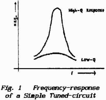 |
For a so-called high-Q circuit
the shape of this curve is very sharp and narrow and, at the peak-response
frequency, it rises considerably above the out-of-band response. For
a so-called low-Q circuit the curve is flat and broad and fails to rise
appreciably above the out-of-band response.
The high-Q circuit is useful in those amplifier arrangements where the
response is required to be essentially at a single-frequency; for
example in an oscillator. The low-Q circuit is useful where the response
is required to cover a range of frequencies as may be found in a radio
receiver. |
Fig.1 demonstrates the disadvantage of this simple
arrangement in that, while the response of the low-Q circuit may be broad-band,
it offers but little discrimination between the required in-band signals and
undesired out-of-band signals; i.e. its use results in both poor amplification
and poor selectivity.
The behaviour of a resonant circuit as either high-Q or low-Q is determined
by the amount of energy that the resonant circuit dissipates. In
technical terms by the losses or the damping that is present. This energy dissipation
takes place of course in the components which make up that resonant circuit
and so the circuit Q-factor is determined by the quality of the components
from which it is constructed; i.e. by the individual component Q-factors (see Lesson
8 in Fundamentals-1). To manufacture
components of poor quality is not a reasonable option because of considerations
such as reliability and the need to maintain control over circuit behaviour.
Thus the bandwidth of an LC resonant circuit is adjusted by adding a known
amount of loss in the form of a damping resistor.
It is evident from the foregoing discussion that a broad-band response and
high-gain are not compatible and so an alternative to the simple resonant circuit
is required.
8.6.3 COUPLED-CIRCUIT THEORY
Broadband responses are obtained by coupling together several simple LC-circuits. There
are several methods of achieving such coupling but perhaps the easiest to grasp
is that which uses the transformer principle.
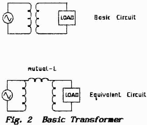 |
Fig. 2 shows
a basic transformer.
The exact mechanism whereby energy is transferred from the primary
circuit to the secondary circuit is not known but it is known that the
amplitude of the secondary signal is dependent on the rate at which the
primary current changes.
At the peaks of the primary-current waveform the current is reversing
sign either from positive-going to negative-going or from negative-going
to positive-going and so, at these points, the rate-of-change is zero.
|
Midway between the peaks where the waveform is crossing the zero line the
rate-of-change reaches a maximum value.
From this can be deduced that the peaks of the secondary waveform coincide
with the zero-crossings of the primary current and that the zero-crossings
of the secondary waveform coincide with the peaks of the primary current; in
technical terms there is a 90° phase-difference between primary and secondary
waveforms.
This phenomenon can be interpreted by saying that the transfer
characteristic (i.e. a comparison of the output-signal with
the input-signal) has the characteristic of a Reactor — there is
a 90° shift in phase as the signal transfers between the transformer
windings. The argument is the same which ever winding is designated
as the primary and so we say that the windings are mutually
coupled. In fact the inter-winding coupling behaves
as though it were an inductor and so it it always represented as a mutual
inductance.
The magnetic field produced by the primary current does not entirely couple
with the secondary winding of a transformer: a proportion of the field
fails to do so and this is referred to as magnetic leakage. Leakage
is expressed as a coupling factor which is given
the symbol k. Should k = 1 then the leakage
is zero; if (say) k = 0. 85 it signifies that only 85% of the
magnetic field is linking with the secondary and as a result the signal coupled
into the secondary circuit is 85% of that otherwise to be expected.
The same argument can be applied to the secondary current and the manner in
which it couples to the primary circuit.
This is a simplified (not entirely accurate) account of transformer behaviour
but it serves to demonstrate that primary and secondary signals are not identical
in Time. Standard textbooks will be delighted to present a detailed analysis
of transformer action in terms of a vector-diagram and one quick look at that
will explain why I do not give such an account here. This inherent
phase-shift caused by the inter-winding magnetic-coupling produces some rather
odd (but useful) results.
If the Load shown in Fig.2 is a pure resistor then
the Generator, “looking- in” through the transformer input-terminals,
sees a resistive load shunted by the inductive-reactance of the transformer
windings. The aim in transformer design is to ensure that this inductive-reactance
has a very-high value at the working frequency and so it can be ignored in
this discussion.
If however the Load consists of a capacitor then the Generator sees an inductive-reactance
while, if the load is an inductor, then the Generator sees a capacitive-reactance.
 |
Fig. 3 shows
a Generator coupled to a Load via a double-tuned transformer; this
basic arrangement is to be found in most receivers. Both primary and
secondary windings are adjusted to resonate at the same frequency (the
method of achieving this is dealt with later).
The frequency of resonance is defined as that frequency at which the
inductive reactance is equal to the capacitive reactance; the two
reactances cancel so leaving both primary and secondary windings purely
resistive in nature. However, it must still be true that the primary
and secondary currents are, relative to each other, phase-shifted
through 90-degrees and so transformer action as described above is to
be expected. |
An Observer who “looks into the primary circuit” in place of the
Generator would see the Load coupled through the transformer action; the Observer
who“looks into the secondary circuit” in place of the Load would
see the Generator coupled through the transformer action.
(a) Frequency Too Low When
the frequency of the generator is lower than the resonance frequency then
the inductive-reactances (in both circuits) fall and the capacitive-reactances
rise; as a result the behaviour of each circuit is controlled by the
capacitive reactance and we say that the circuit becomes predominantly capacitive.
With reference to the previous paragraphs the Generator is presented with
a primary circuit which has a capacitive-impedance plus a coupled secondary
circuit which has been transformed to an inductive-impedance. Similarly
the Load, looking back toward the Generator, is being driven by a secondary
circuit with a capacitive-impedance plus a coupled primary circuit which
has been transformed to an inductive-impedance.
For both primary and secondary windings the change of impedance (from resistive
to capacitive) is modified because the coupled impedance from the other winding
appears to be inductive. Hence the departure from resonance which
might be expected because of the change of frequency tends to be compensated.
(b) Frequency Too High The
same argument applies when the Generator frequency is raised above that of
resonance. Both primary and secondary circuits become inductive but
each couples into the other a capacitive impedance which tends to compensate
the overall impedance change caused by frequency changes.
 |
The double-tuned arrangement
shown in Fig.3 thus tends to remain “in
tune” over a short range either side of the frequency to which
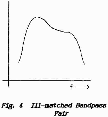
the two circuits are resonated. The extent to which this
self-compensation is successful depends on how well the two circuits
are matched. They must have the same Q-factor and be tuned to the
same centre-frequency; the result of failure in this respect is
shown in Fig. 4.
The bandpass effect depends too on the degree of coupling. It
should be obvious that, if the coupling is too small (i.e. the two circuits
are not coupled), then signal transfer from the Generator to the Load
will not take place. |
As the coupling is increased so the signal level at the load will rise steadily
accompanied by a similar increase in the frequency compensation. It is possible
to make the coupling too tight so that the circuits are over-compensated; when
this happens the circuits are de-tuned off-resonance instead of offering mutual-compensation.
The result of varying the coupling is shown in Fig. 5. Between the under-coupled
single-peak response and the over-coupled double-peak response there is a happy
mean in which the circuit response remains substantially constant over a range
of frequencies. This “flat-topped” condition is termed critical
coupling.
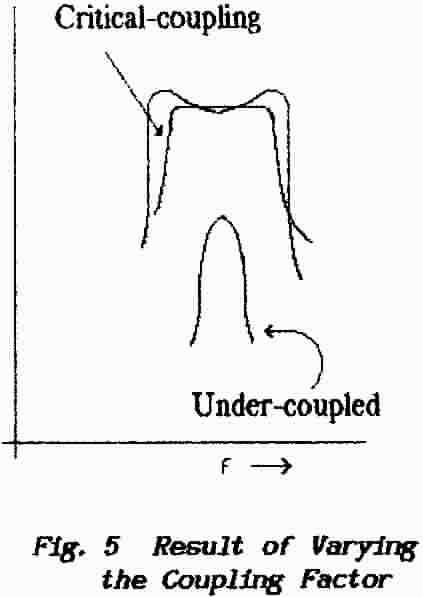 |
It is usual to employ a coupling factor which
is slightly greater than the critical value and this is indicated by
the appearance of two small maxima in the frequency response as shown
in Fig.5.
The amplitude of these bumps is under control as the coupling is increased; the
advantage of this condition is that the bandwidth achieved is slightly
greater than that at critical coupling and also that the skirts of the
characteristic are considerably steeper than with critical coupling. |
8.6.4 OTHER FORMS OF COUPLED-CIRCUIT
The double-tuned--transformer introduced above is
but one way of coupling two resonant circuits. In the equivalent circuit
of Fig.2 two resonant circuits are shown coupled
by a mutual-inductance but this can be reproduced by using any form of reactance
that is common to both circuits; indeed any common impedance will suffice
through which the interchange of energy can take place. Four alternative
arrangements are shown in Fig. 6.
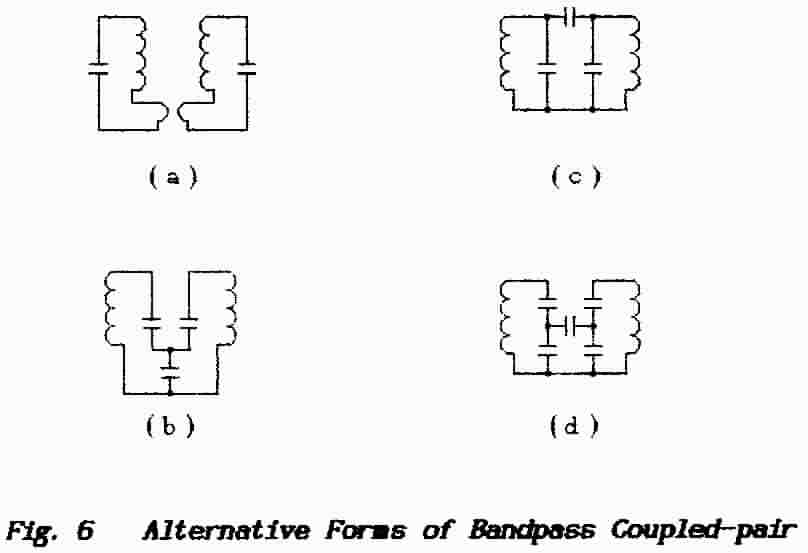
Diagram (a) shows an alternative form of the transformer-coupling illustrated
in Fig.3; this type of circuit was once common
in valve-operated communications receivers where it played a part in arranging
for variable bandwidth in the IF amplifier. Yet another variation occurs where
the “transformer” is replaced by a low-impedance untuned link-coupling
thus allowing the two resonant circuits to be physically separated.
To set-up an inductively-coupled pair they must first be separated so as to
reduce the coupling; when each circuit has been tuned for maximum response
at the desired centre-frequency (fc) then the coils are
moved closer together until the required bandpass characteristic is obtained. The
two coils are then cemented to hold them in position.
Should re-adjustment be necessary it may not be possible to release the cement
and then a different technique is employed. Each circuit in turn is shunted
by a low-value resistor to lower its Q after which the other circuit can be
tuned. However the coupling-factor can only be changed by moving (one of) the
coils.
Diagram (b) shows much the same arrangement but this time each resonant circuit
is tapped in the capacitive arm instead of in the inductive arm. Here the resonance
frequency is determined by Cl and C2 in series while the coupling-factor is
determined by the ratio C2/(C1+ C2). A
difficulty here lies in adjusting the circuit; adjustments to the
tuning or to the coupling are inter-dependent.
Diagram (c) shows a capacitive form of the circuit illustrated in Fig.2 in
which the mutual-inductance-coupling is replaced by a coupling capacitor; sometimes
the required value of this capacitor is impractically small and so the component
is “tapped-down” the circuit as shown in diagram (d). As the tapping-point
is moved down so the circuit impedance at the tap is reduced and thus the required
value of the coupling capacitor is increased. This arrangement can be realised
also by tapping down the inductive branches but it is generally easier to divide
the capacitive arm than it is to arrange for tapings on the coils.
Whether the circuits are tapped in the inductive arm or in the capacitive
arm the same rule applies as for transformer action; the impedance-ratio is
proportional to the square of the turns-ratio or to the square of the capacitance-ratio.
This arrangement is very easy to set up because the coupling capacitor can
be variable. It is set for minimum capacitance (highest impedance and smallest
coupling-factor) and then the two resonant circuits can be individually tuned
to the centre frequency. The coupling-capacitor is then increased in value
until the required band-pass characteristic is obtained.
8.6.5 TO DESIGN A BANDPASS COUPLED-PAIR
As explained in the Lesson notes bandwidth is related to the Q of a circuit
which broadly is the Q of the inductor; this is defined as the ratio Rp
/ Xp, where Rp is the parallel-connected resistance (the
losses) of the circuit.
These circuits are adjusted to be resonant at the centre frequency and so
the value used for X may be that of the inductive-reactance or of the capacitive-reactance.
The following formula relates Bandwidth (ß) in Hz to the values of capacitance
(C in Farads) and resistance (R in ohms) with reference to the circuit shown
in Fig. 7:
ß = √2 / (2π.√C1C2.√R1R2
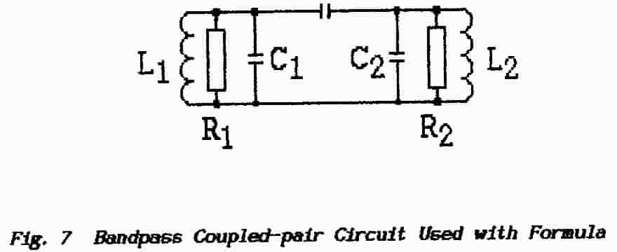
In fact the formula relates to any type of coupled-pair arrangement. It
has been said that an essential feature for a flat-topped characteristic is
that the two coupled-circuits be well matched ; it follows that C1 = C2 and R1 = R2 and
so the formula reduces to
ß = √2 / 2πCR
Compare this with the formula for a single tuned circuit in which ß =
f0 /Q = l / 2πCR
There is a minor catch however in that the values calculated for both C and
R represent the total effective capacitance and resistance in each circuit; this
means that C is formed by the combination of the lumped capacitor and stray-capacitances
and that R is formed by the combination of the lumped resistor and inherent
losses.
The value of C is easily disposed of because the added capacitor has to be
(or to include) an adjustable trimmer. The value required for the additional
resistance however depends on the measured value of the circuit losses; to
determine this either
(i) the coil must be wound, adjusted for approximately the correct value
of inductance and then measured on an Admittance Bridge to
find the value of Rp. The value of the added resistor must then be
calculated to produce, in parallel with the measured value, the required
value of Rp in the above formula
(ii) When a Bridge is not available then the value of R as calculated must
be increased by guesswork and adjusted so as to achieve the designed Bandwidth
when the circuit is finally set-up.
The flat-topped characteristic depends on the coupling between the two resonant
circuits achieving the critical value. This coupling-factor k is
determined from the formula
k = ß/fo = Cc/C
An important parameter when designing a bandpass amplifier is the load which
the coupled pair presents to the active device. This value is the parallel
resistance of R1 and R2. Thus, in
the design of an IF amplifier, the first step is to determine the desired value
of the load and then R1 and R2 are each assigned twice
this required value. Note however that R2 may have to be increased
in value because it will be shunted by the input-resistance of any following
stage.
Back to Top of Page
END OF INFORMATION SHEET 6