** Electrical power is generated and distributed in alternating form for convenience, cheapness and safety but often it is required in direct form. The process of deriving dc from an alternating supply is called rectification and the device which is used to accomplish rectification is called a rectifier. The reverse process, that of obtaining ac from a dc-supply, is known as inversion and the electronic equipment used to achieve it is called an inverter.
** The majority of electronic equipment requires dc-supplies and so, to operate from the normal 240-volt ac "mains supply", a unit must be employed to carry out the operation of rectification, to provide the correct voltage and to provide the necessary smoothing the purpose of which is to remove all traces of ac (see later). This overall equipment is referred to as a Power Supplier.
** There are two approaches to the problem of rectification:
(i) Allow the alternating current to flow in the required direction but prevent it from flowing the other way
(ii) Provide a switching mechanism that will reverse the circuit connections each time the current-flow reverses ; this method has been mentioned already in the mechanical switch of the so-called dynamo (see Fundamentals-1: Mechanical Generators. However, with the mains-supply reversing 50-times every second, a mechanical switch cannot be used and electronic switching is required.
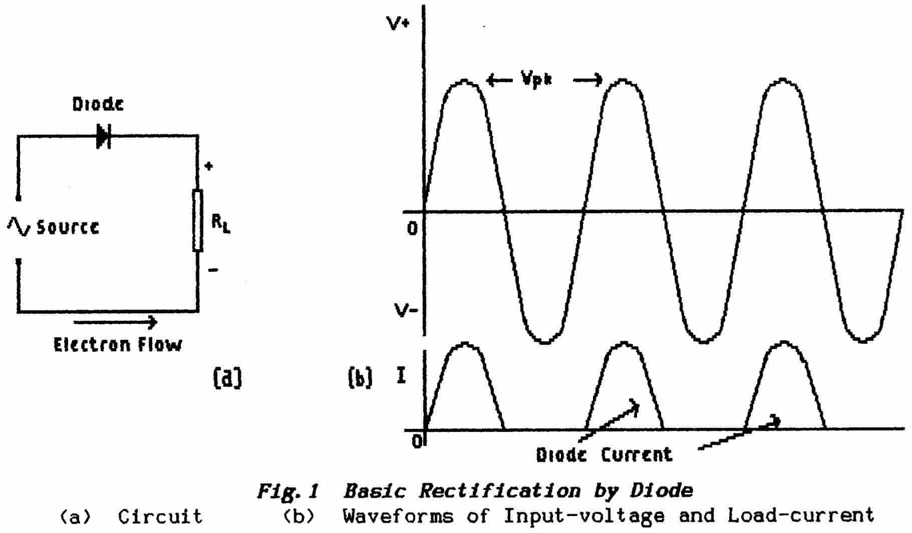
** The first method results in a series of current pulses which occur during alternate half-cycles of the applied emf and the current remains at zero during the intervening periods ; this is known as half-wave rectification and is illustrated in Fig.1.
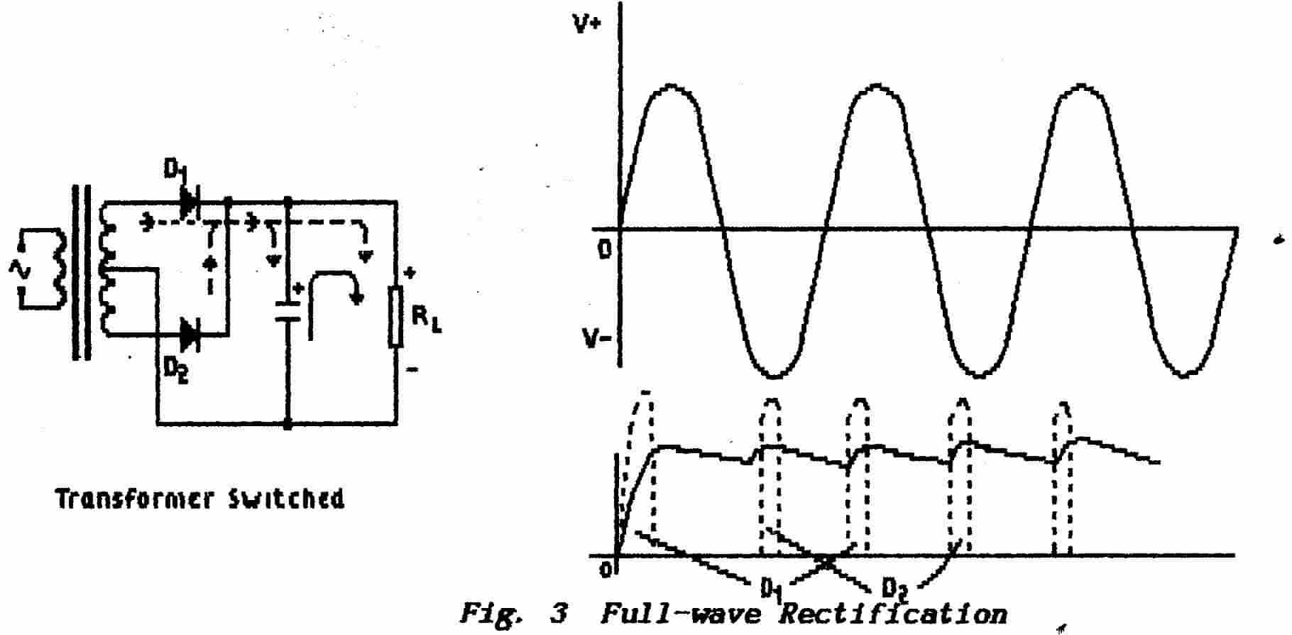
** The second method produces current pulses during each and every half-cycle of the applied emf and is therefore known as full-wave rectification ; this is illustrated in Fig.3.
** Rectifiers are made in both thermionic and semiconductor form ; they have only two electrodes and so are known as diodes. In effect they are switches that are operated automatically according to the direction of current-flow. In one direction they offer between the two electrodes a low resistance to the passage of current but, in the opposite direction, they offer high resistance.
Thermionic diodes, like all valves, contain a heated cathode which emits electrons into an evacuated envelope ; when the second electrode or anode is charged positively with respect to the cathode these electrons are attracted to the anode so forming a flow of electron-current from cathode to anode.
When the anode is charged negatively with respect to the cathode the electrons are repelled back toward the cathode ; the unheated anode does not emit electrons and so a current-flow is not possible. In general valve diodes are useful for rectification above 50 volts.
>>>>>>>>>>>>>>>>>>>> PAGE 2 <<<<<<<<<<<<<<<<<<<<
Back to Top of Page
** Semiconductor diodes do not use a heated cathode but the physics
of their layered internal construction ensures that conduction takes place
in one direction only. These diodes are useful for low-voltage rectification
but there are some types that are capable of working at several hundred volts.
Semiconductor diodes are generally less robust than valve types and must not
be allowed to overheat.
** There is one important difference in that, when a semiconductor
diode is subjected to excessive voltage in the reverse direction, it will abruptly
switch to a second conduction mode ; the voltage at which this takes
place is remarkably constant irrespective of the current which flows and this
is known as the zener voltage of the diode. So-called zener diodes are
manufactured especially for use in this mode ; they have several uses
but the most important is as a reference-voltage source as discussed later.
** Fig. 1(a) shows a diode (general symbol) connected between an ac source and a load represented as a resistor RL. The arrow-head symbol represents the direction of classical-current flow (from positive to negative) and therefore the upper end of RL has a positive potential with respect to the lower end ; semiconductor diodes are marked with a red spot or a line to indicate the positive-output (cathode) connection.
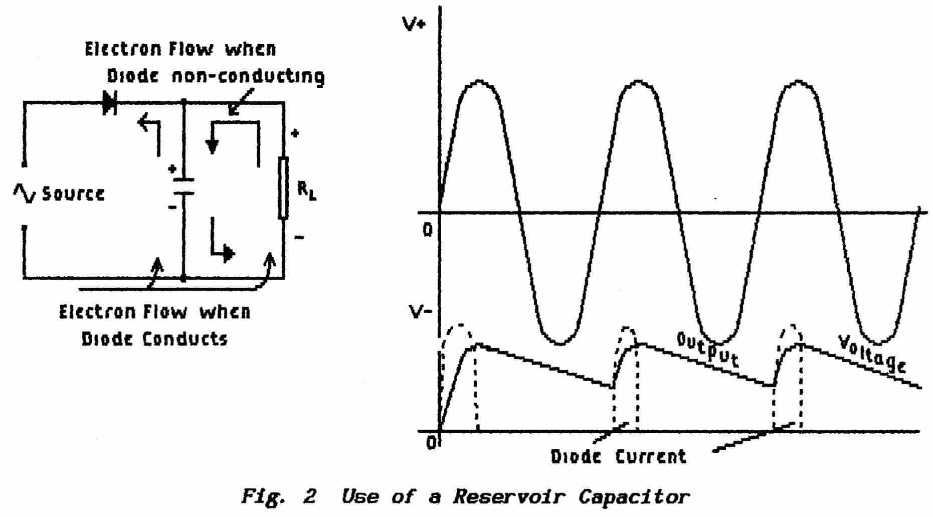
** Fig. 1(b) shows the waveform of a sinusoidal input voltage and the rectified half-wave current that flows through RL. These current pulses spaced at half-cycle intervals are useless as a source of dc and means must be found to keep current flowing during the gaps. The first step in this process is shown in Fig. 2(a) where a large-value capacitor is connected across RL,
** During the half-cycle when the diode conducts there is a flow of current through RL but current flows also into the capacitor and charges it to the peak value of the alternating supply voltage. During the following half-cycle, when the diode is non-conducting, the capacitor discharges through RL so maintaining the load current ; during this process the p.d. across the capacitor falls steadily, as shown in diagram (b), until the emf of the ac-source rises once more and exceeds the residual voltage across the capacitor. Because this capacitor stores charge against future needs it is known as the reservoir capacitor.
>>>>>>>>>>>>>>>>>>>> PAGE 3 <<<<<<<<<<<<<<<<<<<<
** The voltage developed across RL is still not a true direct voltage ; it has a ripple component which will interfere with the operation of electronic circuits. The ripple is removed by filtering techniques described later under Ripple Filters For low-voltage semiconductor circuits this is usually dealt with in stabilising-circuits built into a single chip.
** A full-wave rectifier circuit is shown in Fig. 3 and two obvious requirements are an extra rectifier and a transformer that is wound with a centre-tapped secondary winding. The transformer performs the task of "reversing the connections" ; in fact it provides two alternative feeds which, by virtue of the centre-tap, have opposite polarities. Each diode has its positive-output connection (or cathode) taken to the same end of RL and so, on alternate half-cycles, each drives a pulse of current through the load in the same direction.
>>>>>>>>>>>>>>>>>>>> PAGE 4 <<<<<<<<<<<<<<<<<<<<
Back to Top of Page** A full-wave rectifier circuit produces twice as many current pulses per cycle and the half-cycle gaps are eliminated ; thus, compared with the half-cycle arrangement, the task of the reservoir capacitor is greatly eased. Full-wave rectification offers several advantages:
(a) Improved regulation. A rectifying dc-power supplier has the same limitations as any other source in that, when current is demanded, the terminal voltage falls. The term regulation refers to the amount of that fall with regard to the corresponding current-demand. With reference to Ohm's Law the voltage drop per unit current may be expressed as a resistance in ohms ; alternatively the drop is expressed as a percentage of the off-load voltage when the current is increased from zero to the full rated-value.
A full-wave rectifier delivers twice the number of current pulses and leaves the reservoir capacitor only half the time in which to discharge. Thus its regulation is considerably better than that of a half-wave circuit.
(b) Ripple from a full-wave circuit is much reduced in amplitude because the capacitor suffers less discharge. The frequency of that ripple is twice that from a half-wave circuit. Both factors reduce the demand on the following ripple-filter arrangements which therefore can be constructed either more cheaply or with greater effect.
(c)Because the reservoir capacitor is re-charged twice each cycle and is discharged for a shorter period the pulses of re-charging current which flow through each diode are greatly reduced as compared to the diode-current in a half-wave circuit ; this reduces the cost of the diodes and lengthens their life-expectancy.
Alternatively it allows the value of the reservoir capacitor to be reduced with a consequent saving in cost. However, a reduction of the capacitance must increase the value of the diode current to compensate for the increased rate of discharge.
Yet again reducing the value of the capacitance reduces the initial surge at switch-on as the capacitor charges from zero ; such surges (known as in-rush current) can blow fuses particularly if the moment of switch-on coincides with the ac-input reaching a peak value.
Clearly this is an area where a Designer has to compromise between conflicting factors.
** A disadvantage of the full-wave circuit described above is that it requires a balanced feed ; i. e. it needs two equal supplies of opposite polarity. The centre-tapped transformer which supplies these feeds is specified as (say) 100-0-100 volts and is expensive. The bridge rectifier requires only a single feed and so uses a smaller and cheaper transformer; it can operate also without the need for a transformer. The bridge circuit is also useful where perhaps a centre-tap is not available on an existing transformer.
The arrangement requires four diodes instead of two but this is a reasonable trade. The bridge-rectifier is less suitable for valves because of the need for four separate heater feeds or for well-insulated heaters.
>>>>>>>>>>>>>>>>>>>> PAGE 5 <<<<<<<<<<<<<<<<<<<<
Back to Top of Page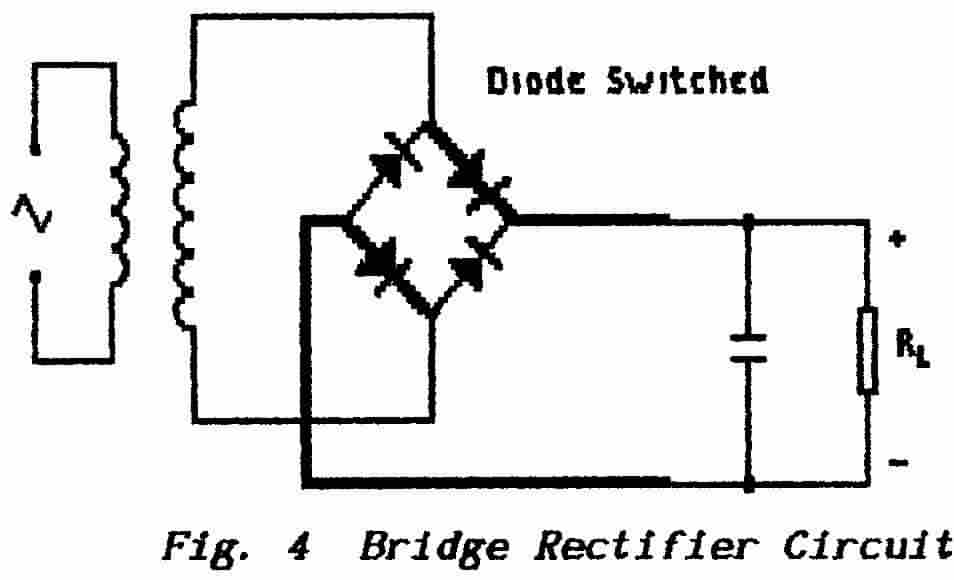 |
** The circuit is shown in Fig. 4 where the heavy lines indicate current flow during one half-cycle of input; the diodes, acting in pairs, interchange the connections each time the alternating supply reverses polarity. ** A disadvantage of the bridge rectifier is that it lacks a common connection between the ac-input to the Bridge and the dc-output and so both cannot be earthed simultaneously. |
These circuits provide full-wave rectification but they produce direct-voltage outputs that are greater than the peak value of the ac-input. They offer also the advantage of a common connection between input and output and so the entire arrangement can be securely earthed. A transformer feed is not necessary.
The disadvantage of voltage-multipliers is their poor regulation. The circuit action moves stored charges between a multiplicity of capacitors and so only small currents can be supplied. Probably their greatest use is in instruments which use small cathode-ray tubes where they supply the e.h.t. (extra-high tension) at around 600 to 1,000 volts with only a few milliamps loading.
Fig.5 shows a voltage-multiplier circuit. In diagrams (i) to (iv) the heavy lines show the circuit action in its first four stages after switch-on; diagram (v) shows the usual presentation which, perhaps more graphically, shows the manner in which charge is boosted step-by-step up the ladder of capacitors switched by a series of diodes.
The principle of operation is that a charge-transfer capacitor is first charged directly from the input ac supply; during the following half-cycle this capacitor is then switched in series with the supply to charge a reservoir capacitor to the sum of the input peak-voltage and the similar p.d. across the charged capacitor. This basic action is extended by adding successive stages of charge-transfer capacitor and voltage-adding reservoir capacitor. The high-voltage output is taken from across all the reservoir capacitors connected in series.
Diagram (i) shows the first charge-transfer capacitor being charged to the peak positive voltage of the input waveform because its right-hand side has been connected to the common earthed line by diode Dl. In diagram (ii) the supply voltage has reversed and diode Dl, now reverse-biased, has become non-conducting. Diode D2 has now connected the input supply in series with Cl across the first reservoir capacitor C4 and so (after several cycles) C4 becomes charged to twice the peak voltage (Vpk) of the supply.
In diagram (iii) both Dl and D2 have become reverse-biased as the supply again reverses polarity. Diode D3 has now connected the charge-transfer capacitors C1 and C2 in series across the supply but, instead of returning
>>>>>>>>>>>>>>>>>>>> PAGE 6 <<<<<<<<<<<<<<<<<<<<
Back to Top of Page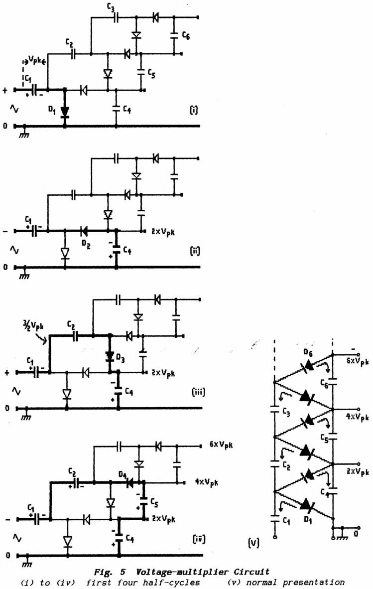
>>>>>>>>>>>>>>>>>>>> PAGE 7 <<<<<<<<<<<<<<<<<<<<
Back to Top of Pagethe connection to the common earthed line, it has taken it to the -2.Vpk potential at the top of C4. The total voltage from which Cl and C2 in series are charging is therefore 3.Vpk . On the fourth half-cycle the two reservoir capacitors C4 and C5 are charged, from the series combination of Cl + C2 + supply, to a total of 4.Vpk .
This process can be continued with each section adding 2.Vpk to its associated reservoir capacitor so increasing the output voltage in steps twice the peak voltage of the supply. Note however that this value 2.Vpk per section is not achieved if charge is lost ; i.e. if current is being drawn from the final output terminal.
A positive output can be obtained from the same circuit by reversing the connections to all diodes.
The arrangement is known as a cascade multiplier. The Designer must pay attention to the voltage rating of the capacitors and diodes. Each reservoir capacitor is subjected to a maximum of twice the input peak voltage and the charge-transfer capacitors should have a similar rating.
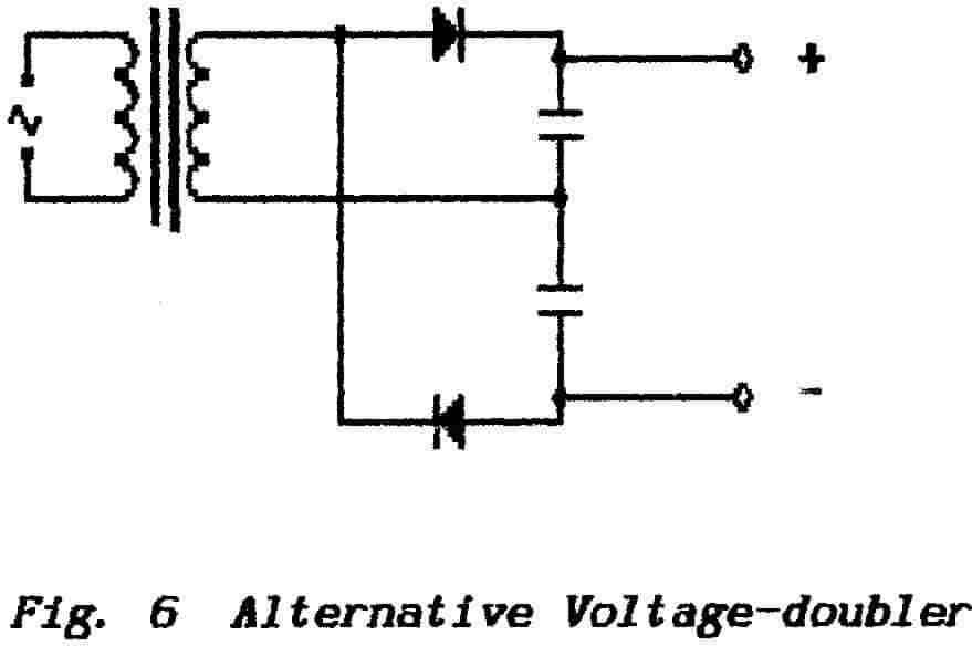 |
There is another form of voltage-doubler circuit which is shown in Fig.6. This uses two diodes to select in turn the alternate half-cycles of an alternating supply; each diode charges its own reservoir capacitor and again the output is taken from across the two capacitors in series. This circuit has the disadvantage of not providing a common earthed connection from input to output and it cannot be extended beyond a multiplication factor of 2; it must be transformer fed. Voltage-doubling circuits are often found in detector stages of a.rn. receivers where they provide a modulating signal of greater amplitude than is obtained with simple diode detectors. |
END OF LESSON 1
>>>>>>>>>>>>>>>>>>>> PAGE 8 <<<<<<<<<<<<<<<<<<<<
Back to Top of PageQUESTIONS
1. Why are Power Suppliers necessary ?
2. Explain the differences between half-wave and full-wave rectifier circuits.
3. What is the basic difference in the purposes of a reservoir capacitor, which is placed at the input to a Ripple Filter, and the smoothing capacitor which is placed at the output of that filter.?
4. What is meant by the term "Regulation" as applied to a Power Supplier?
5. What are the advantages of the full-wave rectifier circuit over the half-wave ?
Where might you expect to use the half-wave arrangement ?
6. Suggest a reason why a bridge-rectifier device is useful in metering circuits such as you might find monitoring the performance of a receiver.
>>>>>>>>>>>>>>>>>>>> PAGE 9 <<<<<<<<<<<<<<<<<<<<
** A stabilised power-supplier provides a direct-voltage output with a value that is maintained at a pre-set or adjustable value irrespective of changes in the load-current or of changes in the supply voltage.
That definition sounds as though stabilised suppliers disobey the "internal resistance" rule that terminal voltage must fall as current-demand is increased but, although they can get very close to doing so, they do not in fact disobey the rule. These stabilisers employ negative-feedback techniques (see under 1.11 Amplification in Fundamentals-1) in which changes in output voltage are measured, amplified and fed-back to a control system that adjusts the circuit to correct those changes. Thus there is a requirement that the output must change if there is to be any control but the magnitude of that change is reduced according to the amount of amplification within the feedback loop.
Depending on the loop-gain and the characteristics of the feedback-loop it is possible for the output voltage to increase with an increase in current-demand and such a circuit could be described as having a "negative output-impedance". This can be a useful facility where, for example, the supply is transmitted over a lengthy run of cable and it is desired to keep the voltage as constant as possible at the delivery point. Such design needs care however if the arrangement is to remain stable.
** Power supplied by Electricity Boards is not supposed to vary
but the unpredictable nature of the demand means that some variation is inevitable. Varying
demands on a supplier arise also from the natural use of the load ; for
example, a transmitter draws a heavy current when keyed but only a small current
in stand-by mode
.
For voltages greater than about 80 volts a shunt stabiliser device would be a gas-discharge valve ; for lower voltages semiconductor diodes are operated in the zener mode which was described in Lesson-1 of this Part.
A gas-discharge device is a diode which does not use a heated cathode but its envelope is filled with a gas at low pressure. A commonly-used gas is Neon and so these valves have acquired the generic name Neons. Electron-flow through the valve is achieved, not by boiling electrons from a heated cathode (thermionic conduction), but by breaking-down the gas into charged components or ions which process is known therefore as ionisation. When the gas ionises and a current flows the gas emits a coloured glow and the valve is said to strike.
Ionisation of the gas occurs at a potential which depends on the gas and on its pressure. However, once ionisation has been effected, the p.d. between the electrodes falls and remains at a (reasonably) constant value irrespective of the current which flows. Circuit design must then ensure that the current remains within the limits set by the Manufacturer. Outside this range the p.d. changes in small but discrete steps.
>>>>>>>>>>>>>>>>>>>> PAGE 10 <<<<<<<<<<<<<<<<<<<<
Back to Top of Page Gas-discharge devices are manufactured to provide
a range of voltages which remain constant within the life of the valve so long
as the current-rating is observed. Thus it is necessary to select both
for the required voltage and for the current-range.
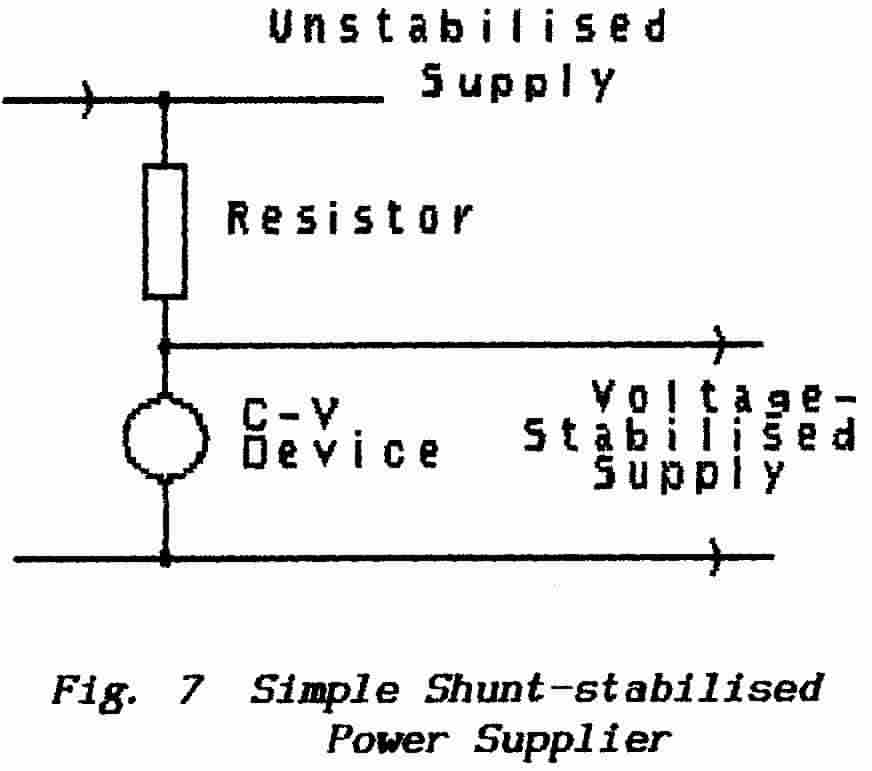 |
** Fig. 7 shows
a circuit arrangement in which either a gas discharge valve or a semiconductor
diode can be used to stabilise the voltage of a small-current supply. The
current through the resistor has two components one of which flows to the
load and the other through the stabiliser. Because the stabiliser maintains
a constant voltage between its electrodes any change in load current is compensated by an opposite change in stabiliser current. The value of the resistor is chosen so that the current through it equals the maximum load current plus the minimum stabiliser current ; should the load current fall to zero it is essential that the stabiliser is able to carry the total current. ** This simple arrangement is frequently used to supply small currents in local parts of large equipments but its capabilities are limited. Should the load-current rise too far then the stabiliser becomes starved of current, ionisation is extinguished and the stabilising action ceases ; should the load-current fall too far then the stabiliser could be damaged. |
A second disadvantage is that it is not possible to vary the voltage at which the output is maintained.
** The output (or source) impedance of the circuit may not be sufficiently low with the result that alternating voltage is superimposed on the dc as a result of an alternating component in the load current. This is usually dealt with by placing a suitable capacitor across the dc output.
However, the parallel combination of a capacitor and a gas-discharge valve can produce an efficient (relaxation) oscillator. An excessive demand f or current extinguishes the valve but the output voltage is unable to rise until the capacitor has been charged. When the output voltage finally reaches the striking voltage of the valve it re-strikes thus increasing the total demand for current which is supplied temporarily by the capacitor. As the capacitor discharges it finally reaches the extinguishing potential of the valve and the cycle repeats. This kind of fault in equipment which has already seen service usually indicates that the gas-discharge device is reaching the end of its useful life.
** The action of this circuit arrangement, in which the stabiliser shunts current away from the load, has given it the name shunt-stabiliser.
>>>>>>>>>>>>>>>>>>>> PAGE 11 <<<<<<<<<<<<<<<<<<<<
** Although resistors R2 and R3 reduce the output voltage as required they also reduce in the same ratio the error-voltage and this degrades the performance as a stabiliser (it degrades the regulation); it is also the reason for requiring amplification in the shunt amplifier. The stabiliser's response to rapid variations is improved by adding capacitor C2 which, by bypassing R2, raises the ac-gain around the feedback loop.
** One likely variation in the output voltage is a residual ripple component from the rectifier circuit which has survived the action of the ripple filter; with the bypass capacitor in place the feedback means that a series-stabiliser can provide a useful improvement in smoothing.
(A considerable improvement in the action of this arrangement can be achieved by re-designing the shunt amplifier as a cascade amplifier but I have not included this design here.)
** Because the object of this arrangement is to deliver a direct supply it is of necessity a dc-coupled circuit and prone to drift problems. The accuracy of the output voltage is dependent on the gain-stability of the series and shunt amplifiers. With a transistor-operated circuit the main cause of gain changes is likely to be changes in the ambient temperature or heat developed in the devices themselves. With valves a major problem is that variation of the ac-supply must alter the voltage of the filament supply.
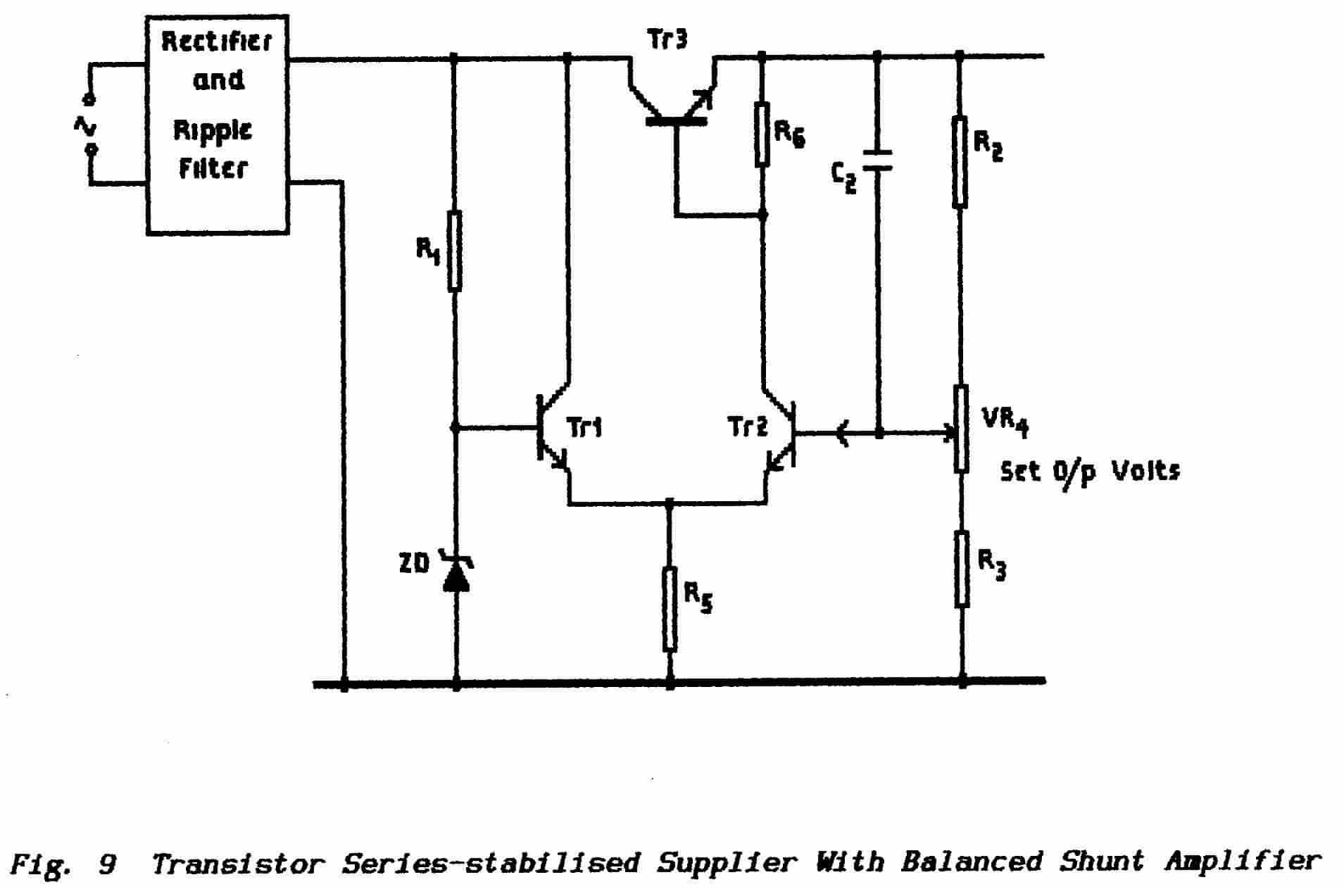
** Fig. 9 shows a detailed transistor circuit in which such
drifts are largely eliminated by use of a balanced amplifier in
the shunt circuit; (see Differential Amplifier in
Part-3, Lesson-2.) The sample-voltage and the reference voltage
are compared in the differential-amplifier Tr1 and Tr2 and the amplified
difference is developed across R6. The intention is that both transistors will
drift in identical manner and so the effects of such drifts will cancel.
>>>>>>>>>>>>>>>>>>>> PAGE 13 <<<<<<<<<<<<<<<<<<<<
Back to Top of Page** In more detail, the reference voltage is developed across the zener diode ZD and transferred by emitter-follower action (see under 3.12) in TR1 across the common emitter-resistor R5 ; the sample output-voltage is applied to the base of TR2 so that the input to this transistor (between base and emitter) is the difference between the two voltages. As an example, suppose that a temperature change raised the base-emitter voltage of the transistors ; the reference voltage across R5 would fall but this would take-up the error caused by the increase in base-emitter voltage of TR2.
Note that the two transistors in the shunt amplifier should be a matched pair and should be mounted in the same way as close to each other as possible.
** Changes in the output voltage at the top end of R2, from whatever cause, are fed only to the base of TR2. and so upset the comparison of reference and sample voltages. Such changes can be deliberately introduced by adding the variable-resistor VR4 which thus enables the voltage at which the output is stabilised to be adjusted.
NOTE Although bipolar transistors
are current-operated it is legitimate to describe the circuit operation in
terms of voltages because the common emitter-resistor provides negative-feedback
which makes both devices voltage-operated.
** In essence these are not different to the series-stabiliser with shunt-amplifier arrangements described above. The integrated-circuit (IC) device embodies the reference-voltage source, the series-stabiliser and the shunt-amplifier transistors in a single small package. They require only the external connection of the rectified ac-supply, the large-value smoothing/reservoir capacitors and (where necessary) a set-volts control. There is a great deal of gain incorporated within the chip and it is often necessary to connect a capacitor of around 330 nF (0.33 μF) directly between the input and common pins to ensure stability.
They differ however in that a separate ripple filter is not usually required and also in that they are far more versatile than the basic circuit using discrete components. They must not be allowed to overheat which means that they must be properly mounted on an adequate heat sink which is a large metal component which will efficiently conduct away the heat and dissipate it into the surrounding air.
(I have twice encountered a vice wherein, for no apparent reason, the device explodes and spreads itself into the far corners of the workshop. I believe this to be caused either by a failure of the heatsinking within the encapsulation of the chip or (most likely) by instability (oscillation) causing local heating: the instability results from omission of the stabilising capacitor .
** Voltage-stabiliser ICs come basically in two kinds namely with fixed or variable output. The variable types offer a pin to which a voltage-control circuit can be connected according to the Maker's specification. However, the fixed types can provide output voltages greater than that specified by use of the circuit shown in Fig. 10(b). (See also 5. 2. 7. Switch-mode. )
>>>>>>>>>>>>>>>>>>>> PAGE 14 <<<<<<<<<<<<<<<<<<<<
Back to Top of Page 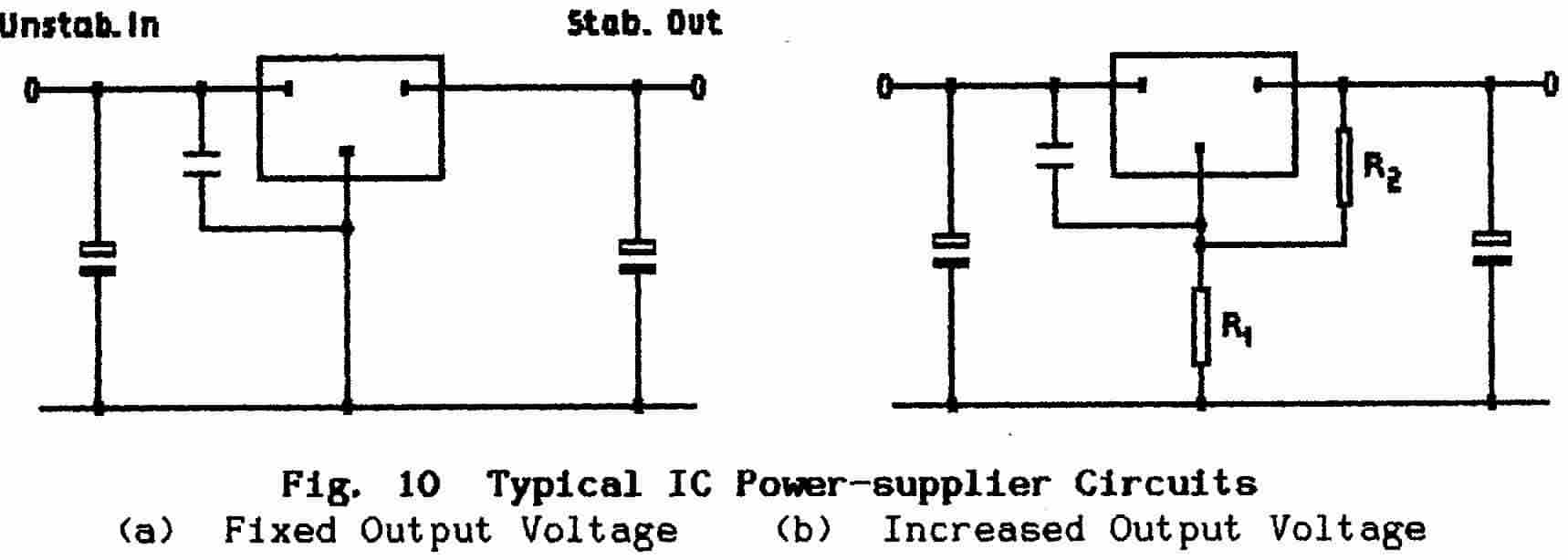
A resistor R1 is connected in the common lead and extra current is bled through this via resistor R2 ; this current should be about 5-times that normally drawn by the IC through its common connection so as to swamp that current. Normal operation of the stabiliser is to maintain a constant voltage between its Output pin and its Common pin and this constant-voltage maintains a constant-current through R2. This constant-current develops a substantially-constant p.d. across R1. The overall output voltage is thus the rated output voltage plus the p.d. developed across R1.
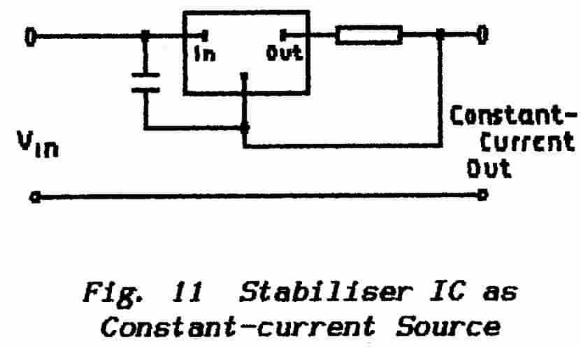 |
These ICs can also be used to provide a constant-current source as shown in Fig.11 . The simplest explanation is once again to note that the IC maintains a constant voltage across the resistor and so enforces a constant-current. |
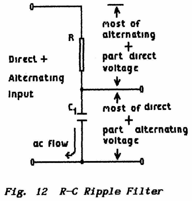 |
** The basic Ripple Filter is shown in Fig. 12 ; it is a potential-divider network in which the lower element is a capacitor. There are different ways of explaining its action but, ultimately, all explanations are the same. (a) at the ripple frequency the low impedance of the capacitor provides a shunt path for the alternating ripple-component and so separates it from the dc which can flow only through the load. (b) the capacitor has a large value so that it needs an appreciable time to charge or to discharge: partial charging and discharging results in only a small proportion of the ripple voltage appearing across the capacitor (which is across the load). |
>>>>>>>>>>>>>>>>>>>> PAGE 15 <<<<<<<<<<<<<<<<<<<<
Back to Top of Page(c) relative to the resistor the capacitor presents a high-impedance to the dc but a low-impedance to the ripple ; this means that the majority of the direct voltage appears across the capacitor (across the load) and the majority of the ripple-voltage appears across the resistor.
** A resistor is not the best component to use in a ripple filter because the dc develops a p.d. across it and that p.d. is dependent in value on the current-demand ; we say that the resistor degrades the regulation. Nevertheless the circuit is frequently used in this form when low current-requirement limits both the voltage drop and the power-dissipation to an acceptable value and the regulation is not of great importance. It provides a very cheap ripple filter.
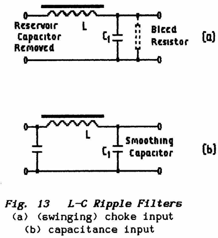
** For large load-currents, or in those circumstances where the current varies widely, it is usual to replace the resistor with an inductor whose function is to offer a high impedance to the ripple current but low resistance to the dc. Ripple has a frequency of 50-Hz for a half-wave rectifier or 100-Hz for a full-wave or bridge type and so the inductor requires an iron core. To prevent the core from becoming magnetically-saturated by the dc it is necessary to introduce an air gap into the magnetic path.
** When, as in transmitters, a large and widely-varying current
is experienced and good regulation is desired it is advantageous to omit the
input (reservoir) capacitor (this capacitor is usually regarded as part of
a capacitive-input filter). Without the reservoir
capacitor the filter is known as a choke-input filter or,
because the rectifier end of the choke is not restricted in its voltage excursions,
as a swinging-choke filter. See Fig.
13(a).
 |
Strictly speaking the
improved regulation of the swinging-choke filter is illusory in that it
results from the fact that the output-voltage under light load does not
reach the peak value of the input waveform.
In practice however the important factor is the variation of the
output voltage and so, provided the reduced (average) output-voltage is
acceptable, then the improved regulation is real enough.
** For proper operation of a choke-input filter it is essential that the load current should not fall below a critical value else the regulation suffers seriously. To this end a bleeder resistor (bleed resistor or bleeder) is sometimes connected across the filter output. |
>>>>>>>>>>>>>>>>>>>> PAGE 16 <<<<<<<<<<<<<<<<<<<<
Back to Top of Page** Those rectifier-IC arrangements which dispense with the series inductor have been the cause of recent legislation. The very-large input capacitor (often as much as 10,000 μF) required certainly reduces the ripple voltage but, as a consequence, it must draw a very large-amplitude narrow pulse of current during the short time which is available to replenish its charge. These large current-pulses load the mains circuit from which the unit is drawing its primary power and cause serious interference in other equipment over a very large radius. In future it will be a legal requirement to fit mains-input filters to prevent this current-spike entering the mains distribution system.
Inversion is the process of obtaining ac from a dc-source and is a necessary first step when, working from battery sources, there is a requirement for supply-voltages in excess of the battery voltage. The dc is first converted to ac, the voltage is stepped up, or down, by means of a transformer and then applied to a rectifier/filter system as described above.
Three methods of dc-to-ac conversion are available:
(a) chopper
dc is interrupted by either electronic or mechanical means thus converting it to a squarewave in which the amplitude represents the value of the direct voltage. After voltage-transformation this is rectified as described above.Today such interruption is accomplished by some form of gate circuit which is driven by a locally-generated gate-drive waveform.
This system is the basis of the chopper-type dc-amplifiers (see Part-3) for which a synchronous detector is essential to preserve the polarity of the dc-signal. The synchronous detector is basically another gate circuit which is driven by the same gate-drive waveform that serves the chopper circuit.
In early equipments a mechanical vibrator was used to chop the dc and a secondary set of contacts on the same vibrator served as the synchronous detector.
(b) oscillator
with the advent of low-voltage power transistors it is possible to construct an oscillator to work directly from the low-voltage dc source. A transformer-coupled oscillator is used (see Part 4) and the transformer is provided with a high-voltage winding which is then used as the source for a rectifier unit. In such a circuit the ac-waveform is a sinewave.This type of circuit is often found in units which use cathode-ray tubes.
(c) motor-generators
are seldom seen nowadays. Basically the battery source is used to drive an electric motor which is mechanically-coupled to a generator; the generator provides either ac or dc supplies as required. A motor-generator is a machine in which the armature is double-wound ; one winding is used to drive the machine as a motor while the other acts as a generator. A motor-generator set consists of a single motor mechanically coupled to several different generators on the same shaft.Back to Top of Page
>>>>>>>>>>>>>>>>>>>> PAGE 17 <<<<<<<<<<<<<<<<<<<<
These units, usually referred to as "switchers", provide very compact and reasonably-light power-suppliers but they are most complex in their design and construction and hazardous for the unskilled or unwary serviceman.
The incoming ac-mains supply is applied directly to a bridge-rectifier thus eliminating the bulky mains-transformer. The resulting full-wave-rectified dc is roughly smoothed with a capacitor-filter in which neither side is earthed. BEWARE.
This dc is then switched across the input to a transformer which has multiple windings that, via individual rectifier circuits, provide various supplies as required. The switching (or chopping) is carried out by means of a squarewave-driven power transistor.
One of the dc outputs is sampled to provide an error-signal which is fed-back to the oscillator circuit to maintain control over the output level. This is achieved (for example) by varying the mark-space ratio of the squarewave (pulse-width modulation).
A large part of these power suppliers consist
of safety circuits which (for example) shut-down the unit in the event of excessive
load current. One odd feature is the so-called kick-start mechanism.
The squarewave generator and its associated control circuits require dc supplies
which are not available until the oscillator has started to oscillate. At
switch-on the rising dc from the rectifier is made to charge a capacitor and
this, with a trip circuit, starts the oscillator and then effectively removes
itself from circuit.
A similar technique is used in the integrated-circuit switching-regulators which increasingly are replacing the linear regulators described under 5.2.4. In use these require considerably more external components but they have the advantage that the output voltage can be greater than or less than the input voltage provided that the total device power-dissipation is not exceeded.
Their mode of operation is similar to that of the coil-ignition circuits used in motor cars . The input direct-current flows through an inductor and is switched at a frequency around 100 kHz by means of a square-wave oscillator; when the current is interrupted the voltage developed across the inductor charges a capacitor via a blocking diode . A variable resistor varies the mark-space ratio of the switching squarewave and this sets the output voltage.
A disadvantage is that the switching-oscillator can cause problems with e.m.c. and care is required in construction.
END OF LESSON 2
END OF PART 5