Home Page Lesson
2
PART 4: ELECTRONIC OSCILLATORS
LESSON 1
4.1 THE DAMPED OSCILLATION
As described in Lesson 9 of Part-1 resonance
results when two energy stores are coupled together. In electrical circuits
the two components concerned are a capacitor and an inductor and the energy
is interchanged between the electrical field of the capacitor and the magnetic
field of the inductor.
Practical circuits however also possess resistance
to the flow of current and this results in heat-generation which represents
a loss of energy from the circuit. There are other losses too such as heat
which develops in the dielectric of the capacitor and energy lost through radiation
(other than heat) but these are generally small compared to the
"ohmic" losses.
** Without such losses a perfect circuit,
which would be constructed from a "perfect" inductor and a
"perfect" capacitor, would continue to oscillate for ever once it
had been energised. The practical circuit however loses an amount of energy
each time there is a flow of current.
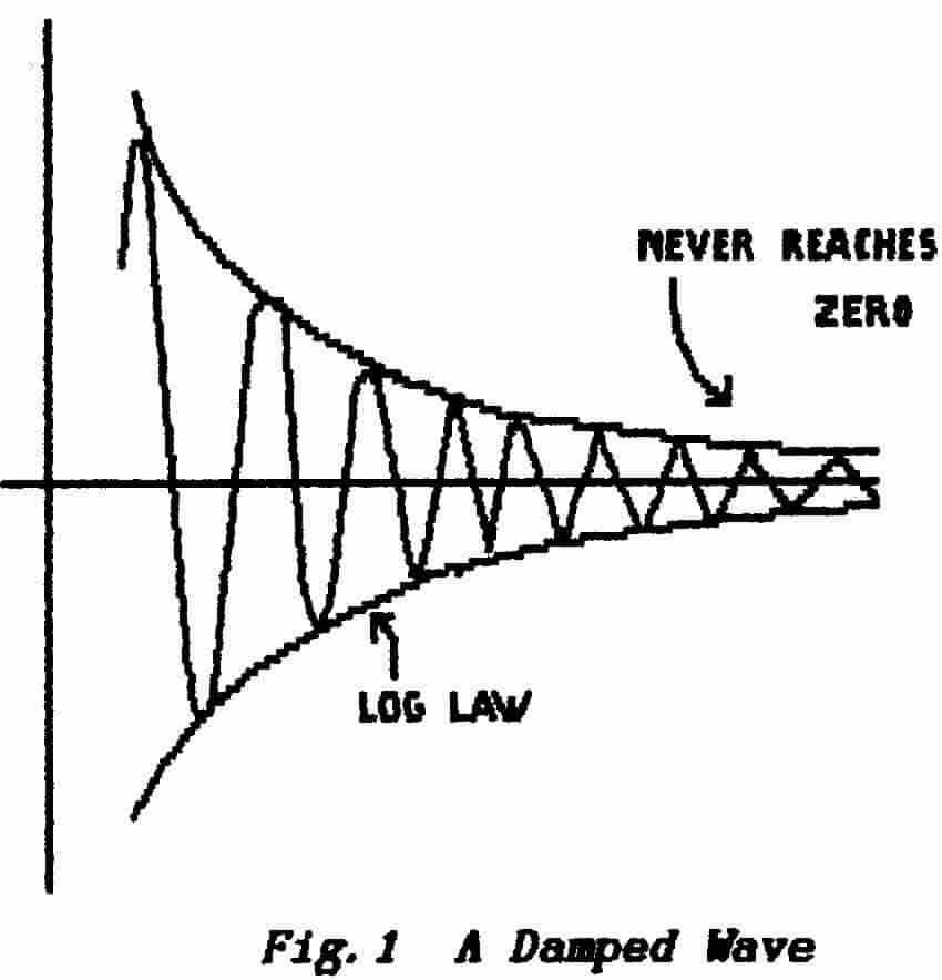
It follows that each cycle of oscillation must be smaller than the previous
cycle and this is shown in Fig. 1 . A resonant
circuit which loses energy in this manner is said to be damped (the
term is an exact analogy with the similar act of
"damping" a bell) and so the series of waveforms as illustrated is
referred to as a damped-train.
 |
In each cycle the current which flows through the inductor is a function
of the voltage which appears across the capacitor ; at the end of each
cycle the capacitor acquires a slightly lower voltage because of the
ohmic losses. The losses themselves are a function of the magnitude of
the current.
This argument shows that the losses in each
cycle are dependent on the magnitude of the previous cycle and also determine
the magnitude of the cycle which is to follow ? |
This phenomenon, in which what happens next
is determined by what has just happened, is an example of a logarithmic
law (see 7.2 in Part-7 Mathematics). The envelope of the decaying
wave follows a logarithmic curve and so we say that the waveform suffers an exponential
decay. As with all logarithmic functions you may
take any two consecutive cycles and the ratio of their peak values will always
be the same. This is another way of saying that the decay from one cycle to
the next is always the same percentage decrease. (With
other mathematical laws the decrease might be (say) a constant percentage of
the starting value.)
>>>>>>>>>>>>>>>>>>>>
PAGE 2
<<<<<<<<<<<<<<<<<<<<
The Spark Transmitter mentioned in Lesson-1
of Part-2 radiated a continuous train of these damped oscillations because
the means were not then available to overcome the damping effect of the circuit
losses. Thus it was necessary to constantly re-charge the resonant
circuit so as to generate a waveform which could be radiated from an aerial.
4.2 MAINTAINED OSCILLATION
4.2.1 Use of Feedback
As mentioned above a continuous oscillation is possible if the circuit losses
can be eliminated.
In fact this is possible using so-called cryogenic techniques to
take the conducting material down to a very - low temperature (close to Absolute
Zero) when it becomes superconductive - i.e.
virtually electrically lossless. The exact meaning of this is made clear perhaps
by considering a superconducting store (memory). When a loop of wire is/rendered
superconducting and a current pulse is induced into it that pulse propagates
round and round the loop endlessly without dissipating its energy. Powerful
superconducting electromagnets remain cool because the electric coils do not
dissipate energy.
However, maintaining cryogenic equipment is not a practical way to make an
oscillator. At normal temperatures the circuit losses cannot be eliminated
but it is possible to eliminate their effect. To do this it is necessary
to introduce a small amount of energy to replace that dissipated in the circuit
resistance. In Part 1 it was mentioned also that this first became possible
with the invention of the triode valve.
Consider a resonant circuit which loses 10%
of its contained energy with each cycle of oscillation. A signal, taken from
that resonant circuit, is passed through an amplifier with a power-gain of
1.1 (i.e. 10%) and then returned to the resonant circuit ; each cycle of oscillation
now has the same magnitude as the previous cycle. The output from the amplifier
has been used to boost the input signal and so this is an example
of positive feedback.
Should the gain of the amplifier be too small,
then the oscillation will die away; it will take longer to decay
than would the same circuit without the amplifier but it would decay nonetheless.
If the gain of the amplifier stage is too large then each cycle will be of
greater magnitude than its predecessor ; i.e. the oscillation will build-up.
The last effect will not necessarily
lead to disaster because, as the oscillation amplitude increases, so too will
the 10% losses and eventually a condition could be reached in which oscillation
is once more maintained at a constant (but larger) amplitude.
Clearly a control mechanism is required that is capable of adjusting the amplifier
gain. If the oscillation amplitude begins to increase then the amplifier
gain must be decreased slightly ; if the oscillation amplitude begins to
decrease then the amplifier gain must be increased slightly. Given this automatic
control of amplitude then the circuit can be maintained in continuous and
steady oscillation.
>>>>>>>>>>>>>>>>>>>>
PAGE 3
<<<<<<<<<<<<<<<<<<<<
Back to Top of Page
There are several devices which can perform this control function and they
all operate within a negative-feedback loop. The
oscillation-amplitude is monitored and an error-signal is generated which
describes the manner in which the output deviates from the required amplitude
; this error-signal is then used to adjust the gain of the maintaining amplifier.
The most common form of control loop is an automatic-bias circuit. The maintaining
device is allowed to pass a current which is proportional to the amplitude
of the oscillatory signal and this charges a capacitor; the voltage across
this capacitor is then used as a bias to reduce the amplifier gain. When
the oscillation amplitude increases the capacitor is charged to a higher
voltage ; when the oscillation amplitude decreases the capacitor voltage
falls as the capacitor
In devices such as precision signal-generators,
where the Designer has tried to avoid the waveform distortion which is inherent
in automatic bias circuits, you may find more expensive solutions. Some of
the output power from the oscillatory circuit may be fed to a thermocouple which
generates a small voltage that is proportional to the temperature of a two-wire
junction. Alternatively a small heater may be used to adjust the resistance
of a heat-sensitive device or, today, the resistance of a semiconductor device
may be adjusted by means of a small light-emitting diode which is fed with
the oscillator output. Needless to say these circuits are slower in their reaction
to amplitude disturbances.
4.2.2 Frequency Stability
To understand the mechanism which keeps an
electronic oscillator to a single frequency it is necessary to examine the
resonant circuit more closely. Fig. 2 is a graph
which shows the changes of impedance presented to a generator by a parallel
combination of inductor and capacitor.
 |
At low frequencies the capacitor is virtually open-circuited and all
the signal current flows through the inductor. The reactance therefore
is a very-low positive value. As the frequency rises toward the right-
hand end of the graph so the reactance increases as shown. (See Lesson-6
of Part-1.)
At very high frequencies the inductor is virtually open-circuited and
all the signal current flows through the capacitor. The reactance
therefore is a very-low negative value. As the frequency falls toward
the left-hand end of the graph so the reactance increases toward
a high negative value. (See Lesson-7 of Part-1.) |
>>>>>>>>>>>>>>>>>>>>
PAGE 4
<<<<<<<<<<<<<<<<<<<<
Back to Top of Page
At the centre of the graph we have to create
a continuous curve by joining together the high positive reactance of the inductor
and the high negative reactance of the capacitor ; as shown this results
in a very abrupt transition. Note that, if we choose a large inductor and small
capacitor , this transition will be much more abrupt than if we use a small
inductor and large capacitor. However the maximum values of impedance will
be limited by the circuit losses which appear as a parallel-connected resistor.
Thus while the sharpness of this transition depends on the values chosen for
the L and C it is critically dependent on the circuit Q-factor (see Lessons
8 & 9 in Part-1).
** The important point is that, when the circuit oscillates exactly
at its resonance frequency, then the overall reactance is zero (wL -1/wC)
which corresponds to the point where the abrupt part of the curve crosses the
zero line. Should the frequency rise then the reactance very-rapidly becomes
capacitive ; should the frequency fall then the reactance very-rapidly
becomes inductive. It is the resultant rapid shift in the phase-relation between
applied voltage and resulting current which controls the behaviour of the positive-feedback
circuit.
** Very-high-Q circuits (low-loss circuits) present transitions that are very
steep indeed. Thus oscillators which use high-Q circuits are constrained to
keep within very-narrow frequency limits. (See Fundamentals-2, Lesson-1,
Page 4)
4.2.3 RC and Crystal Oscillator
Circuits
** As an introduction to oscillator circuits the LC oscillator
is probably the easiest to follow. However, all that is required is a positive-
feedback circuit to make good the natural circuit losses (and losses due to
signal-extraction), a negative-feedback circuit to control the amplitude of
oscillation and a phase-sensitive circuit to act as a frequency-controlling
device.
A series or parallel combination of inductor
and capacitor is the most obvious choice but phase-sensitive networks can be
created from either a combination of resistance and inductance or from a combination
of resistance and capacitance.
These two families each have two forms
(a) the reactor in series and the resistor in shunt (b) the reactor
in shunt and the resistor in series. As a rule-of-thumb series-capacitor circuits
are used where the phase-shift network doubles also as a RC-coupling between
amplifier stages.
 |
Shunt-capacitor and also inductive
networks find their uses in current-driven stages (e.g. bipolar-transistor
maintaining amplifiers).
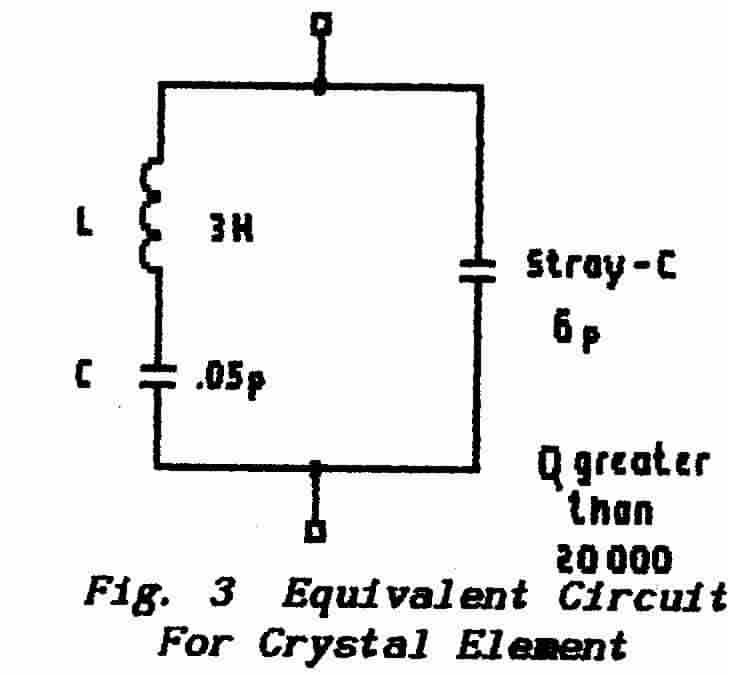
** Fig. 3 shows the equivalent electrical circuit for a
slice of quartz crystal which has been cut and mounted for use in controlling
an oscillator. The crystal itself behaves like a series combination
of Land C and this is shunted by a small capacitance which results from
the crystal
mounting. Typical values are given in the diagram. |
>>>>>>>>>>>>>>>>>>>>
PAGE 5
<<<<<<<<<<<<<<<<<<<<
Above the natural resonance frequency of the
crystal the controlling (series) reactance is inductive and this resonates
with the parallel stray capacitance to produce a secondary resonance. It is
important to recognise three factors:
(a) The lower of the two resonance frequencies is a series mode and therefore
the crystal is working at low impedance
(b) The higher of the two resonance frequencies is a parallel mode and therefore
the crystal is working at high impedance
(c) Stray capacitances form part of the parallel-mode circuit and so a parallel
crystal is ground to work with a specified capacitance.
I have met many instances of crystal oscillators producing the "wrong" frequency
and there are many people who believe that a crystal-oscillator can only
operate on its "correct" frequency. Investigation
has shown that either the wrong crystal has been inserted, a crystal calibrated
for series operation is being used in a parallel-mode circuit, a crystal calibrated
for parallel operation is being used in a series-mode circuit or that a parallel-crystal
is being used with shunt stray-capacitance other than that originally specified.
** In a circuit operating with a parallel crystal it is possible to
connect a small variable trimmer-capacitance across the crystal to provide
a fine adjustment to frequency. It should be remembered that this trimmer belongs
to the crystal and not to the circuit, that it should be used to set the crystal
on the specified frequency and that the crystal cannot give of its best if
any other frequency is used. Such a trimmer can operate over a limited range
only and will not be effective in a series-mode circuit.
** Oscillators should always be driven as lightly as possible; i.e.
just hard enough to ensure reliable operation. A maintaining amplifier which
is overdriven will distort the waveform and thus destroy the frequency stability.
A distorted waveform indicates the presence of harmonics which, in turn, requires
the resonant circuit to increase its bandwidth i.e. the circuit Q has been
lowered. Alternatively you may prefer to consider that an over-driven amplifier
is likely to draw excessive input current, which corresponds to a fall in input
resistance which adds excessive damping to the resonant circuit ; once again
the circuit Q is degraded.
** Note that, if the bias circuit time-constant is made too large,
then the charge on the capacitor cannot leak away fast enough and oscillation
ceases. Oscillation restarts once the bias has decayed sufficiently. The result
is a series of short bursts of oscillation — a performance known as squegging.
4.3 OSCILLATOR CIRCUITS
4.3.1 The T.A.T.G. Oscillator
The tuned-anode-tuned-grid oscillator
gets its name obviously from the early days of its use with valve maintaining-devices.
Not only is it possibly the simplest of the oscillator circuits to understand
but it is probably the most commonly-encountered circuit — usually without
intent.
Back to Top of Page
>>>>>>>>>>>>>>>>>>>>
PAGE 6
<<<<<<<<<<<<<<<<<<<<
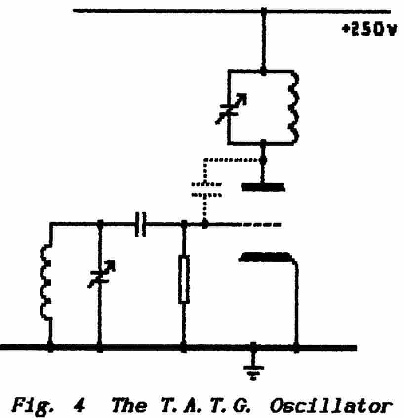 |
Fig. 4 shows the circuit in its valve form using a triode.
It consists of two tuned LC circuits, one in the anode and the other in
the grid, which are coupled via the anode-to-grid stray capacitance. Sometimes,
and especially at low frequencies, it is necessary to increase this
feedback capacitance by adding an external component.
The grid circuit is the frequency determining
element ; the anode circuit needs to be tuned to a slightly lower
frequency so that the anode load appears to be inductive.
This offsets the phase-shift caused by the capacitive feedback path and
so ensures that, at the desired resonance frequency, the feedback is
entirely positive. |
The simplicity of the circuit comes at a price.
The need to tune the anode circuit to a different frequency means that the
tuning elements cannot be ganged. Additionally ganging would not be easy because
both sides of the anode capacitor are at 250 volts. It is possible to connect
the anode capacitor between anode and the negative line, thus allowing the
tuning shaft to be at ground potential, but this means that the capacitor has
to withstand the sum of the h.t. supply plus the peak oscillatory voltage (up
to twice the h.t. potential).
The grid frequency-determining circuit can
be replaced by a crystal operating in its parallel mode and the result is a
very reliable and flexible oscillator. This t.a.t.g. valve circuit was frequently
used in a pentode arrangement in which the screen-grid acted as the oscillator
anode and this allowed the anode-circuit to be tuned to the second or third
harmonic of the crystal. Such an arrangement provides excellent buffering for
the oscillator ; i.e. the oscillator is protected from loading by the output
circuit. This and similar circuits are known as electron-coupled oscillators.
The circuit, though seldom used today, is of
importance in that it is often created unintentionally. For example, a multi-stage
rf or if amplifier consists of several amplifier-stages separated by tuned
(or double-tuned) circuits. If one of these circuits is set to a too-low frequency
and there is sufficient gain available, the entire "amplifier" will
turn abruptly into a t.a.t.g. oscillator (see Lesson-5 in Part-3),
Note the grid-coupling capacitor and grid-leak resistor
shown in Fig. 4. The valve is not
provided with automatic cathode bias and so the positive-going half-cycles
of input voltage drive the grid into drawing grid current. This current charges
the coupling capacitor and so drives the grid negative which lowers the stage
gain. This charge continually leaks from the capacitor via the resistor and
is replenished every half-cycle. Thus any increase in oscillation-amplitude
increases the bias while any decrease in oscillation-amplitude allows the bias
voltage to decrease. If this grid combination is removed and replaced by an
automatic cathode-bias circuit the oscillator will not function.
>>>>>>>>>>>>>>>>>>>>
PAGE 7
<<<<<<<<<<<<<<<<<<<<
END OF LESSON 1
* * * * * * *
* * * * *
QUESTIONS
1. What is the prominent characteristic of a damped oscillation ?
2. How does an active device turn a damped oscillation into continuously-maintained
oscillation?
What else is required to ensure continuous oscillation?
3. Why does such an arrangement prefer to operate at a single frequency ?
4.Give reasons why a crystal oscillator may NOT operate at the frequency which
is printed on the crystal casing.
5. What adjustment must you make before a T.A.T.G. oscillator will burst into
song ?
What is probably wrong if the oscillator produces bursts of oscillation instead
of a continuously-maintained waveform ?
6. Given the crystal constants shown in Fig. 3 calculate the (series) resonance
frequency of the crystal. Use reasonable approximations to avoid complicated
arithmetic.
Can you indicate the method of calculating the parallel-resonance frequency
? You need an algebraic solution; if your maths do not run to this exercise
can you at least show the way ? (Not for the R.A.E.)
>>>>>>>>>>>>>>>>>>>>
PAGE 8
<<<<<<<<<<<<<<<<<<<<
Back
to Top of Page
LESSON 2
4.3.2 The Transformer-coupled Oscillator
The simplest way to feed the output of an amplifier-stage
back to its input is by means of a transformer. Where the oscillation is maintained
by a valve or by a field-effect transistor the transformer must feed back a
voltage-sample of the output ; where the oscillation is maintained by a bipolar
transistor then the transformer must feed back a current-sample of the output.
The difference is significant. The input-impedance
of a valve or of a FET is very high and so a step-up (voltage-gain) transformer
is required (see Lesson-5 in Part-1). The input-impedance of a bipolar transistor
is very low and so a step-down (current-gain) transformer is required.
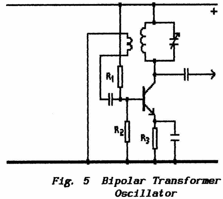 |
As in the t.a.t.g. circuit
the control of oscillation-amplitude can be left to an automatic grid-bias
(base-bias) circuit . If the transformer is resonated it will also provide
the necessary phase-sensitive network to control frequency-stability. Note
that, to achieve stable single-frequency operation, the transformer must
be single-tuned i.e. not bandpass-tuned.
** The result is shown in Fig. 5 where
a bipolar npn transistor is used. The collector winding has
been resonated because it is the high-
impedance winding and so requires the smaller capacitance. The choice
of time-constant for the base CR combination is dependent on the frequency
of oscillation. Increasing the time-constant (with frequency unchanged)
increases the base bias and so reduces the amplitude of oscillation.
(Note that the value of R is obtained from the parallel-combination of
R1 and R2. )
|
As before it is necessary not to drive the amplifier too hard and, where
appropriate, it is important not to saturate the iron core of the transformer.
In a valve maintained version it is the grid
which is resonated and the result is known as a Meissner Oscillator.
It is not so easy to use a MOSFET device as an oscillator
because its insulated gate does not draw current and so an automatic bias circuit,
as described above, is not possible. Other methods are available but these
are not examined for the R.A.E.
>>>>>>>>>>>>>>>>>>>>
PAGE 9
<<<<<<<<<<<<<<<<<<<<
The Hartley Oscillator (and the Colpitts described
next) is a natural development of the transformer oscillator in that it uses
a single tapped coil as an autotransformer (see Lesson-5 in Part-1). The
basic circuit is shown in Fig. 6 ; diagram (a)
gives the straightforward form and
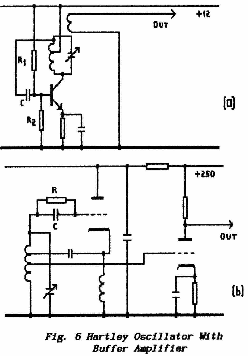 |
diagram (b) a so-called inverted form.
The advantage of the inverted Hartley is that the various components
can be isolated from the supply voltage which is an important consideration
in high-voltage valve circuits.
Note the use of a resistor-capacitor decoupling
circuit to prevent feedback from the buffer amplifier to the oscillator.
The buffer amplifier is shown with an untuned
load thus avoiding the need for a twin-ganged tuning capacitor. Greater
isolation of the oscillator may be obtained by operating the buffer stage
at either the second or third harmonic of the oscillator frequency but
this is practical only with fixed-frequency operation unless two tuning-controls
are acceptable.
In diagram (a) the dc-supply is fed to the transistor through the windings
of the inductor and this arrangement is referred to as a series-fed
oscillator. In the inverted form of diagram (b)
the dc-path has been diverted from the coil which is capacitively-coupled
to the valve;
the choke provides a dc-path in parallel with the oscillatory circuit
and so this arrangement is referred to as an inverted shunt-fed or parallel-fed Hartley
oscillator. |
By careful design a Hartley circuit can be
electrically-balanced so that the frequency of oscillation is substantially
unaffected by the parameters of the active device and this can greatly increase
its frequency stability.
Clearly this circuit cannot be adapted for
crystal-control.
Back to Top of Page
>>>>>>>>>>>>>>>>>>>>
PAGE 10
>>>>>>>>>>>>>>>>>>>>
4.3.4
The Colpitts Oscillator
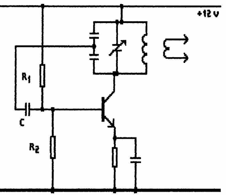
Fig. 7
A Colpitts Oscillator |
One version of this circuit is illustrated in Fig.7. It
differs from the Hartley only in that, instead of using a connection to
the inductor, the tuned-circuit is tapped in its capacitive leg.
This circuit too can be constructed in both normal and inverted forms
and can be either series-fed or shunt-fed.
Inspection of the circuit shows that the internal
capacitances of the active device are in parallel with the two parts
of the tuning capacitance ; variations in the active device can thus
cause frequency drift and it is essential that the tuning capacitors
greatly exceed the values of the strays. |
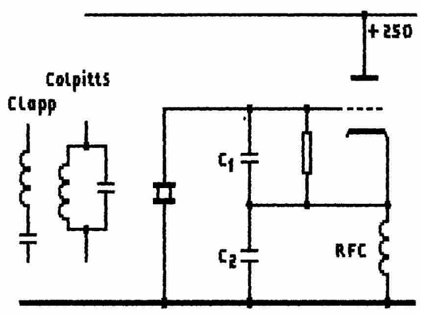
Fig. 8 A Crystal-controlled Colpitts
or Gouriet Oscillator
|
Fig.8 shows
the Colpitts adapted in its inverted shunt-fed form for parallel-mode crystal
operation.
There are hidden traps waiting for the unwary. The coupling capacitors
Cl and C2 provide a tapping across the crystal but, acting together, they
also form extra capacitance across the crystal ; this extra capacitance
must be accounted for when specifying the crystal parallel resonance.
The values of Cl and C2 would likely
be in the region of 100 pF ; if these are increased to values around 1,000
pF the circuit turns into a Clapp/Gouriet oscillator and will jump to the
series-resonance mode of the crystal (see next Section). Unless well designed
this arrangement is not a very good bet therefore unless you have a need
for an oscillator that might jump erratically between modes. |
>>>>>>>>>>>>>>>>>>>>
PAGE 11
<<<<<<<<<<<<<<<<<<<<
Back to Top of Page
4.3.5 The Clapp or Gouriet Oscillator
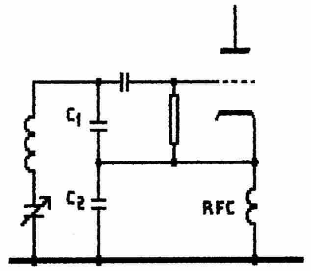
Fig. 9 The Clapp/Gouriet Oscillator |
This circuit was developed
specifically as a very-stable drive for MW-transmitters. It was developed
in this country during the second world-war by G.G. Gouriet who could not
publish his results for security reasons.
It was also developed by Clapp in America.
The circuit seeks to eliminate the drifting
effects of the maintaining device by using very-large value capacitors
to tap into the resonant circuit. To do this the LC circuit is
used in its series-resonant mode.
Particularly in its crystal-oscillator
form the circuit regularly appears with small coupling capacitors ; this
overdrives the crystal and, apart from destroying its frequency-stability
and accuracy, can cause destruction of the crystal. Another common
fault is the failure to realise that,
properly-designed in this Clapp/Gouriet arrangement, the crystal will
oscillate in its series-resonant mode. |
4.3.6 The Pierce Oscillator
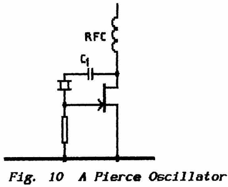 |
This circuit uses the phase-sensitive
arrangement in series with the positive- feedback path and hence it too
uses a series-resonant mode.
In Fig. 10 a Pierce Oscillator is shown using
a crystal and a JFET. In this circuit the crystal capacitance
combined with the resistor to ground, form the biasing CR. The capacitor
Cl serves to protect the crystal from the supply voltage. The radio-frequency
choke (R.F.C.) could be replaced by a resonant circuit. |
4.3.7 Resistance-capacitance Oscillators
In the previously-described oscillators the
positive-feedback path was maintained via an LC resonant circuit which produces
an exact p. f. b. only at the resonance frequency. A similar frequency-sensitive
circuit can be obtained however by a network of resistors and capacitors ; these
fall roughly into two classes:
(a) circuits which produce 1800 phase-shift
(b) circuits which produce zero phase-shift.
>>>>>>>>>>>>>>>>>>>>
PAGE 12
<<<<<<<<<<<<<<<<<<<<
Back to Top of Page
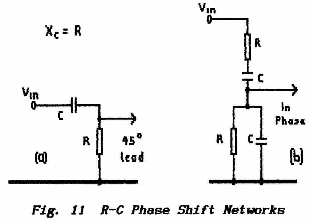 |
Fig. 11 shows examples of each circuit and both depend
on the fact that the current which flows through a capacitor leads
the voltage across that capacitor by 900.
In diagram (a) a resistor is connected in
series with the capacitor. With respect to the common current the voltage
across the capacitor leads by 90° while the voltage across the resistor
is in phase with the current.
The value of the capacitor is chosen so that,
at the required frequency, the reactance is equal to the resistance ;
draw a vector diagram and you will see that this results in the output-voltage
being phase-shifted by 450 with respect to the input-voltage. |
In theory two such R-C sections should give
an overall phase-shift of 900 but, of course, practical components
have losses and so the phase-shift must be slightly less than 450.
For this reason it is usual to use three sections and operate at 600 per
section thus giving a margin for error. To make an oscillator with this arrangement
an amplifier stage is required that both inverts the signal (1800 phase-shift)
and makes good the attenuation through the three-stage RC network.
In diagram (b) a series RC network is employed
together with a parallel RC network in a Wien Bridge circuit. The
current which flows through the series circuit is divided between the two arms
of the parallel circuit which produces a 450 voltage phase-lag so
that the overall phase-shift is zero. To make an oscillator with this arrangement
an amplifier is required that does NOT invert the signal but which makes good
the attenuation through the R-C network. To do this with normal discrete amplifying
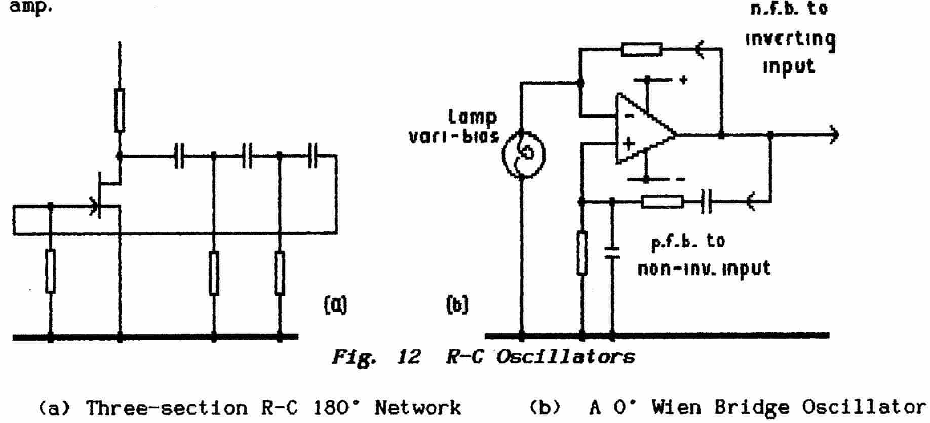
stages a 2-stage amplifier is necessary but Fig. 12(b) shows
a neat way of achieving an oscillator using the differential inputs of an op-amp.
>>>>>>>>>>>>>>>>>>>>
PAGE 13
<<<<<<<<<<<<<<<<<<<<
Back to Top of Page
As explained under 3.11 &
3.13 an op-amp has two differential inputs of which one produces an in-phase
output signal while the other produces an anti-phase output signal.
Feedback via the Wien-bridge circuit is applied to the in-phase (+) input thus
achieving a p.f.b. loop. Feedback to the other (-) input produces a n. f. b.
loop which controls the gain through an automatic-bias circuit. This
utilises a filament lamp as a temperature-variable resistor whose resistance
increases as the current through it increases and so, by increasing the bias,
decreases the stage-gain.
4.3.8 Relaxation Oscillators
These are oscillators which, essentially, have
too much uncontrolled gain around the positive-feedback loop and this causes
them to generate excessive bias which shuts-down the amplifier. The bias, stored
as a charge in a capacitor, then leaks away through a resistor (the circuit
is said to relax) until the amplifier gain is sufficient
to support oscillation when the cycle repeats.
The first of these circuits is the Blocking
Oscillator which, essentially, is a transformer-coupled oscillator
as illustrated in Fig. 5. The automatic
base-bias (grid-bias) time-constant is made too large for continuous oscillation
with the result that the circuit performs a one-half-cycle oscillation
and then remains quiescent for a period determined by the time-constant.
The output from such an oscillator consists of a series of large-amplitude
pulses separated by relatively-long periods of time. They often find use
in driving time-bases for picture-monitor tubes perhaps because they are
easy to synchronise to an external waveform.
The second type of relaxation oscillator is
the multivibrator. This uses a 2-stage amplifier
in which the output of each stage is coupled to the input of the other thus
creating a positive-feedback loop with considerable gain. Again an automatic-bias
circuit is employed with a large time-constant that rapidly generates a bias
but only allows that bias to leak away slowly. The output from these oscillators
is a rectangular wave with very rapid transitions between the full supply value
and near-ground. This lower level is approximately 50-volts in valve-operated
circuits.
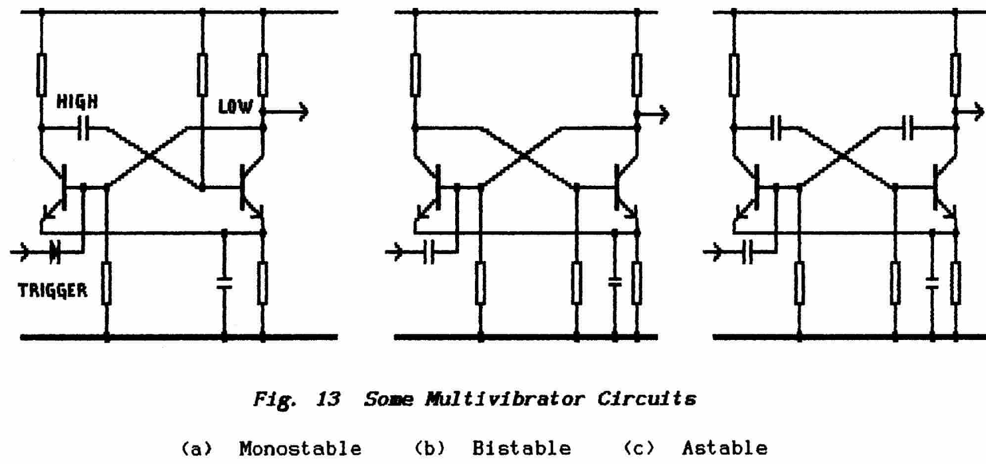
Multivibrators are found in an almost endless
variety of forms but they all fall into the three categories namely monostable,
bistable and astable. Monostable forms have one direct-coupling and one RC-coupling
and, as a result, they have one state in which they remain stable ; e.g. with
amplifier-1 cut-off and amplifier-2 bottomed (fully-on). When triggered
these m.v.'s switch into the alternative unstable state (amplifier-1 bottomed,
amplifier-2 cut-off) and remain there for a period determined by the RC time-constant
before reverting to the stable state. They are used mainly for generating time-delays.
Bistable m.v.'s are dc-coupled and have
two stable states ; when triggered they switch to the alternative state and
remain there until triggered again. These are the basis of the binary counting-circuits
described in Part-2, Lesson-4.
The astable forms are entirely RC-coupled and
so are without a stable state ; when powered, they constantly change
between the two possible states ; these are often referred to as free-running
multivibrators.
Some examples are given in Fig. 13.
>>>>>>>>>>>>>>>>>>>>
PAGE 14
<<<<<<<<<<<<<<<<<<<<
Back to Top of Page
4.3.9 The Timer Chip 555
The 555 is a very versatile - even famous -
chip that, although basically a timer, can be used for an almost endless variety
of tasks. Indeed its possibilities form the subject of several books. The 8-pin
chip contains a monostable multivibrator, two voltage-comparators, an output
amplifier and a couple of other inputs and outputs. By varying its connections
and changing external components it can be used as an oscillator, a timer,
a pulse generator, a pulse-position modulator — to name but a few. It
has a sister chip the 556 which, with 14 pins, offers two separate 555 units.
The basic chip costs around 35p and is an ideal
device on which the newcomer to electronics can try his hand at practical construction.
4.3.10 Harmonic Oscillators
This may appear to be a somewhat obscure title
but it refers to oscillators which produce an output at a frequency which is
greater than the natural resonance frequency of the frequency-determining circuit. In
general such oscillators are suitable only for fixed-frequency working.
There are two basic techniques employed:
1. The oscillator-unit is a multi-stage device in which the first stage is
an oscillator and the following stages act as frequency-multipliers thus producing
an output which is a harmonic of the oscillation frequency.
2. An oscillator circuit is arranged to have considerable gain at the required
harmonic of the frequency-determining circuit so that oscillation takes place
at that harmonic frequency and so suppresses the fundamental mode of oscillation.
>>>>>>>>>>>>>>>>>>>>
PAGE 15
<<<<<<<<<<<<<<<<<<<<
Back to Top of Page
The first type is referred to as an oscillator
and multiplier chain and indeed the oscillator stage may
employ a circuit of the second type. Each stage must be resonated at the
frequency at which it is to operate and it is this requirement which makes
it difficult to construct the device as a VFO.
Note that the frequency-multiplication also multiplies any frequency drift
of the fundamental oscillator.
In valve circuits the technique was often used
in the so-called electron-coupled oscillators which provide isolation between
the fundamental oscillator and the following stages. The oscillator stage uses
a pentode valve in which the screen-grid is pressed into service as the anode
of a triode; this part of the valve forms the fundamental oscillator. Its
operation "modulates" the electron stream that passes
through the screen-grid to arrive at the anode. The anode circuit is resonated
at the desired harmonic frequency - usually 2nd or 3rd harmonic — and
it is driven by the modulated anode-current. The excellent isolation
between output and oscillator arises from the difference in their frequencies
of operation.
** The second type of harmonic oscillator is most usually a crystal-controlled
type in which the crystal is specially cut to make it active at the desired
harmonic frequency. Such a crystal is labeled with the frequency at which it
is intended to operate but it is easy to spot because that frequency is above
the normal range of crystals. But beware ! The harmonic crystal is capable
of sustaining oscillation at its fundamental frequency and confusion results.
I have been confronted with a frequency synthesiser
which refused to produce a variable output so that the output remained fixed
no matter how the frequency-control was set. Both oscillators were operating
powerfully and, at first, I took it for granted that the crystal oscillator
was on the correct frequency. When, in desperation, I checked it with a wavemeter
I found it to be having a Ball at the fundamental; i.e. one-third of the frequency
marked on its case. The cause was low current-gain (about 1/3rd) in the maintaining
transistor. [A likely explanation is that there was insufficient gain to maintain
the 3rd-harmonic mode of oscillation, that this resulted in low-bias on the
transistor which therefore exhibited a too-large input capacitance;
in turn this modified the oscillator circuit so that there was sufficient gain
for the fundamental mode to take over. If this is true it indicates that
the design of the oscillator was faulty.] The problem was cured
by simply exchanging the transistor.
The above is not an exhaustive list of
oscillator arrangements but contains most of those likely to be met in amateur
radio. The only ones likely to be examined for the R.A.E. are the Colpitts
and the Hartley but even then not in any detail. However, if you buy elderly
valve-operated gear, you might well meet any of these except the 555.
END OF LESSON 2
END OF PART 4
Back to Top of Page