Fig. 1 The Diode Valve
In this Part of the Course the discussion moves on to the technical details of radio and electronics circuits and by far the greater part of these are amplifiers. There are many types of amplifiers and many ways of designing and constructing each of those types and so, before delving into their internal workings, it is a good idea to define what each type is and its intended purpose.
While reading the following paragraphs however do bear in mind that many specific amplifiers fall into several different categories either simultaneously or because, without particular alteration, they can perform several different tasks. Some of the differences may also be little more than a matter of definition.
An electrical signal can be measured by either of its two parameters namely voltage or current; where both are present with reasonable amplitude then the circuit is handling power.
A voltage amplifier is one which increases the amplitude of the voltage component but takes little, if any, account of the current; by reference to Ohm's Law such an amplifier operates at high impedance.
A current amplifier is one which increases the amplitude of the current component but takes little, if any, account of the voltage; by reference to Ohm's Law such an amplifier operates at low impedance.
A power amplifier is required to supply a signal to some power-consuming device such as an aerial or a loudspeaker and so it must be able to increase the amplitudes of both the voltage and current components simultaneously. An amplifier which deals in power must itself dissipate power (see Maximum Power-transfer Theorem end of Lesson 11 in Fundamentals-1) and so is in danger of overheating.
(There is an unfortunate mix-up in terminology in that a constant-voltage amplifier (see Lesson-11 in Fundamentals-1) may sometimes be referred to as a voltage source meaning that that particular amplifier maintains an accurate waveform for the voltage component irrespective of any current distortion. A constant-voltage amplifier is of course a voltage-amplifier also but it is not necessarily true that one designed to amplify the voltage component maintains a constant-voltage output. As explained in the Lesson on Internal Resistance it is a matter of the relation between amplifier output-impedance and the Load.]
As a general rule - though not by any means a strict rule - valves operate at high impedances and so amplify the voltage component while transistors operate at low impedances and so amplify the current component. By various circuit tricks and the use of the different kinds of feedback techniques it is possible to make valve current-amplifiers and transistor voltage-amplifiers.
>>>>>>>>>>>>>>>>>>>> PAGE 2 <<<<<<<<<<<<<<<<<<<<
Power amplifiers can be constructed from either valves or transistors but valves are much more rugged than transistors (or other semiconductor devices) and will survive considerable abuses where semiconductors are often destroyed instantly by the heat generated.
Both valves and transistors require that their various connections be held at specific direct potentials and that they draw specific direct currents; these supplies are purely to maintain the device in the condition required for it to function as the required amplifier. Often a change in dc-conditions will convert the one device into several different classes of amplifier.
The vast majority of signals handled by electronic equipment have alternating waveforms and these are superimposed on the direct potentials and currents; the required alternating output signals are recovered by separating dc and ac through the agency of devices which will pass only alternating currents ; e.g. capacitors and transformers.
However, requirements do arise to:
(a) amplify small changes in direct potentials or currents (for example in making measurements such as temperature and pressure)
(b) amplify signals whose frequency range goes all the way down to zero-frequency - or dc. Perhaps the most well-known of these is a video signal which is the total electronic signal that describes a picture.
(Note: a vision signal is an rf-carrier which is modulated by a video signal: a television signal is the combination of a vision signal with the corresponding sound-carrier modulated with the sound-signal.)
The various ac components of a video signal describe the changes in relative brightness (the picture details) along each line of which the picture is composed; a direct component describes the amount of white light present apart from any detail information. This dc-component defines the difference between a high-key (bright) picture and a low-key (dark) picture.
Clearly an amplifier which relies on capacitive or transformer couplings cannot pass on such dc information and it is a purely ac-amplifier.
A dc-amplifier however is a little more subtle. As used in thermometry to amplify the temperature-dependent output from a thermocouple the amplifier would amplify only dc and, in particular, a slowly-varying dc; it would be described as having a narrow bandwidth (perhaps only a few Hz starting from zero) because detailed information is not present.
A video amplifier which handles a picture signal as it comes perhaps from a television camera, may have a bandwidth that extends from zero (dc) up to 5 MHz or even greater. It would be described as having a wide bandwidth.
Both the above amplifiers are described as dc-amplifiers not because they amplify direct signals but because they use dc-couplings (direct-couplings) as distinct from capacitive or transformer ac-couplings. The term means that each stage of amplification is connected directly to the next so that the dc-conditions
>>>>>>>>>>>>>>>>>>>> PAGE 3 < <<<<<<<<<<<<<<<<<<<
are passed on from stage to stage as well as the ac information. Needless to say the technique brings some problems particularly with valves which require fairly high-voltages.
The greatest problem with dc-amplifiers is drift mainly caused by temperature changes. Reasonably small changes in dc potentials and currents do not affect the performance of an amplifier as such but clearly, where the dc-potential is itself the information signal, then drift is a matter for concern. A common solution to this problem is to chop the direct signal with a square-wave (a gate-circuit is opened and closed regularly by a square-wave signal) thus turning the direct signal into an alternating one whose amplitude represents the magnitude of the dc. This ac-signal is then amplified free of drift problems in an ac-amplifier and finally turned back into a direct signal. Such an amplifier is referred to as a chopper-amplifier.
A wide-band so-called dc-amplifier can be used to amplify ac signals. A good example of this perhaps is in an oscilloscope. The spot on the screen of an oscilloscope is deflected by applying a voltage waveform between the appropriate pins of the tube. Direct potentials are required to position the spot but an ac-amplifier is required to raise the signal voltage to the several hundred volts required to form the waveform picture. A dc-amp is often used for this job; it acts as a straightforward amplifier as far as the input signal is concerned but, by juggling the dc conditions within the amplifier, the position of the picture on the screen can be controlled. There is a bonus in that, because the amplifier is dc-coupled, the oscilloscope can measure direct as well as alternating waveforms.
The definition of these two classes is obvious but deceptively so. As explained under 1.14.2 in Lesson 10 of Funds.-1 there is a relation between bandwidth and the speed at which a waveform changes. For example, when a cw-transmitter is keyed, the resulting Morse characters have sharp edges in which the carrier-amplitude first rises and then falls abruptly. Such edges generate high-order harmonics with considerable amplitude and so the signal would spread interference throughout a large part of the radio spectrum. The introduction of a (key-click) filter to remove these harmonics results in the amplitude-changes taking place more slowly.
Thus a wide-band amplifier can handle signals which change amplitude rapidly while a narrow-band amplifier can handle only those signals which change amplitude slowly.
The difference is important in control systems where feedback loops abound. For example, in an a.g.c. system the a.g.c. line is heavily filtered (or decoupled) and this produces a slow response; this is useful in that it prevents the a.g.c. from arguing with the stages whose gain it controls which process could produce an effect of fading where signal-fading is not occurring.
(A good example of the difference between wide-band and narrow-band systems is found in the human body. The semi-circular canals of the inner ear are usually represented as organs of balance; experiments show that they have a bandwidth of several octaves and so must have a fast response. In fact the canals do not tell us that we are falling but how fast we are falling. They constitute an accelerometer.
>>>>>>>>>>>>>>>>>>>> PAGE 4 <<<<<<<<<<<<<<<<<<<<
By contrast the bandwidth of the eye is a small fraction of an octave and so its response must be slow. Your eye will certainly tell you that you are falling but the information arrives too late to be of much use; the function of the eye is to tell you exactly where you are. This slow-speed response is exploited hilariously by some boxers and wrestlers who, by slowly swaying their body, cause an opponent's attack to miss them completely.
** As described briefly in Fundamentals-1 the feedback technique takes a sample of the output from a system and feeds it back to the input where it is mixed with the normal drive signal. Positive-feedback loops are to be found in amplifier designs but the subject is not a matter for this Course.
In a negative-feedback loop the feedback sample is mixed with the input signal in such a way that it tends to cancel that input signal. One of its greatest assets is that it also tends to cancel any distortion that is introduced by the amplifier. For this reason a n.f.b. audio-amplifier tends to produce a "cleaner" sound than one without feedback but all too often the technique is abused. It is a strict rule that n.f.b. can be used to make a good amplifier better but it cannot be used to make a bad amplifier good. In fact, the application of n.f.b. to a poorly designed amplifier can lead to disastrous results; you have every right to be suspicious when you see the phrase " ... cleaned-up by the application of feedback..."
The discussion in Lesson 11 of Fundamentals-1 shows that the relation between a source and a load determines the operation of electronic circuits. For example; in driving a bipolar-transistor amplifier, where input-resistance changes with the signal waveform, it is essential to preserve the current waveform. This requires that the source of the driving waveform should be a constant-current device; the source impedance must greatly exceed the transistor input-impedance. This is arranged by the judicious use of n.f.b. either on the transistor in question, on the source circuit or on both circuits. (Note that the base current that flows to the transistor must be controlled by the source-resistance and NOT by the varying base-input resistance.)
BUT, if an amplifier has a natural bandwidth which extends only to 5 kHz and this has been "extended" to 7 kHz by the application of feedback, trouble is bound to ensue. The apparent extension of the bandwidth has arisen because the n.f.b. has reduced the in-band gain; as the gain falls away from 5 kHz to 7 kHz so too does the n.f.b. It follows therefore that, from 5 kHz to 7 kHz, the output impedance too changes and the amplifier performance becomes progressively inferior.
** Negative feedback is applied to amplifier systems to:
1. Reduce distortion
2. Stabilise the gain (ac feedback)
3. Stabilise the dc-conditions (dc-feedback)
4. Stabilise the circuit against changes of active device (valve or transistor) which may occur through ageing, replacement following failure or changes in ambient temperature.
>>>>>>>>>>>>>>>>>>>> PAGE 5 <<<<<<<<<<<<<<<<<<<<
5. Stabilise the circuit against the ageing/temperature changes of other components such as resistors, capacitors and diodes
6. Control the phase response
7. Adjust the input impedance
8. Adjust the output impedance
9. Adjust the frequency response by weighting the feedback loop; this term refers to placing filters in the feedback loop to make its effects variable with frequency. (Note that this practice affects also all the items above.) A low-pass filter placed in an amplifier will remove the high frequencies; the same filter placed in the feedback loop removes the n.f.b. at high frequencies and so increases the gain at high frequencies.
The fact that a single feedback loop operates simultaneously all nine of the above factors indicates the complexity that can arise.
The term very-low frequencies refers here to the range below normal hearing say from zero to around 30 Hz. In this range inductive and capacitive elements are not practical arid so amplifiers required to operate here would almost certainly be dc-coupled as discussed under 3.4
** An audio amplifier covers the range of frequencies normally distinguished by the human ear say 50 Hz to a maximum of 16 kHz. Voice frequencies are defined as those essential for the transmission of speech of commercial quality, often referred to as telephone quality and covering the range 330 - 3,400 Hz. The full bandwidth is sometimes described as "music quality".
The full range from 50 Hz to 16 kHz is enjoyed only by the young. In noisy environments the upper range falls away with increasing age and often the upper limit is around 6 or 7 kHz.
Amplifiers which cover the full range are known colloquially as high-fidelity (or hi-fi) amplifiers and, usually, are capacitively or inductively (transformer) coupled. They use n.f.b. to reduce distortion and to provide an output impedance that damps any mechanical resonances in the loudspeaker.
A video amplifier is used to handle picture signals either for television purposes or other displays such as computer outputs. Their bandwidth extends from zero frequency up to around 10 MHz maximum depending on the definition required in the displayed picture.
Such amplifiers may be dc-coupled, may use an approximate method of replacing the dc-component after amplification known as dc-restoration or use an accurate method of replacing the dc-component known as clamping; this matter is not required for the RAE. In valve-operated video amplifiers the high-impedance and shunt capacitances of the valves make it very difficult to obtain these very-wide bandwidths; transistors on the other hand, although intrinsically offering greater capacitances, are low-impedance devices and the usual problem is to restrict the available bandwidth to that required; frequency-weighted n.f.b. loops are the usual means of achieving this limitation.
>>>>>>>>>>>>>>>>>>>> PAGE 6 <<<<<<<<<<<<<<<<<<<<
It is necessary to restrict bandwidth because this reduces the generated noise but also because it removes the possibility of spurious oscillations occurring.
** Radio-frequency Amplifiers, as used here, indicates all amplifiers which handle signals above the audio range. This definition excludes video amplifiers which extend downward to zero frequency. They are mostly tuned amplifiers which use either simple circuits or bandpass circuits.
** Wideband rf-amplifiers is a term which usually refers to an untuned rf-amplifier and this uses a simple resistive load; because the stray capacitances are not eliminated by incorporation into a tuned circuit they shunt the resistive load and so tend to restrict the bandwidth. The only cure is to choose a low value for the load resistor and this means that such amplifiers usually offer low gain; mostly they are used to buffer one circuit from another.
** These definitions refer to the mode in which amplifiers operate as determined by the dc-conditions.
** Class-A Amplifiers are biased to the centre of their normal operating range so that the direct current drawn from the auxiliary supply can be either increased or decreased by the same amount. This mode gives the least distortion and is the one used for most voltage or current amplifiers. It is used frequently too for small power amplifiers but results in the least efficiency - such an amplifier gets very hot.
** Class-C Amplifiers are biased so that, without an input signal, they do not draw current from the auxiliary supply - they are said to be normally cut-off. In fact they are biased well beyond the cut-off point. An input signal drives a Class-C active-device into conduction during a small part of one half-cycle only and so greatly distorts the waveform; as a consequence it can be used only in some form of (un-modulated) rf-amplifier where a tuned circuit can be used (like a flywheel) to restore the output waveform. The benefit however is greatly-increased efficiency.
** Class-B Amplifiers are biased half-way between the Class-A and Class-C modes and effectively amplify one half of the input waveform without too much distortion. As a result it is necessary to construct Class-B amplifiers using two active devices such that one amplifies one half of the waveform and the other device amplifies the other half of the waveform. Such an arrangement is referred to as a push-pull amplifier.
** The two halves of the waveform are usually reconstituted by use of a special transformer. This technique is used for efficient high-power audio amplifiers where a single-ended Class-A amplifier would cause heating problems. With semiconductor devices it is possible to build transformerless push-pull output stages.
** There is an arrangement which falls between the Class-A and Class-B circuits known as Class AB. As might be expected such an amplifying stage is not biased for Class-A operation but it is not so heavily biased as to take it into Class-B; various options are available between the two extremes and, depending on the degree of biasing, they are designated ABl, AB2, etc.
>>>>>>>>>>>>>>>>>>>> PAGE 7 <<<<<<<<<<<<<<<<<<<<
** All Class-AB and Class-B amplifiers cause some distortion and negative feedback is used to restore the waveform after everything possible has been done, by design and adjustment, to minimise that distortion.
** These classes of amplifiers have been covered already in the above Sections. Transformer-coupled designs use a transformer to couple the output of one amplifier stage to the input of the next thus preventing the dc in the output from upsetting the dc-conditions at the input of the following stage. Designing these transformers for full-bandwidth amplifiers is a job for the expert.
** The RC-coupled amplifier uses capacitors to block the dc between stages but it is necessary to supply a high-resistance path to enable the capacitor to both charge and discharge with the signal waveform. The combination of resistance and capacitance in the coupling has given its name.
The coupling circuits however begin to fail with falling frequency as their time-constant (see Lesson 3) becomes comparable with the time of one cycle (the periodicity of the signal). With several RC circuits in cascade throughout the amplifier the resulting fall-off (or roll-off) in frequency can become so rapid that (with feedback applied) phase-shift troubles can lead to instability. This has to be countered by staggering the time-constants; i.e. using a different combination of capacitor and resistor for each coupling circuit.
As already described direct-coupled (or dc) circuits do not use coupling networks but connect the output of one stage directly to the input of the following stage. Usually, to maintain the necessary dc-operating conditions, this involves the use of some kind of potential-divider network together with extra biasing lines or the inclusion of semiconductor diodes to adjust the dc potentials.
END OF LESSON 1
* * * * * * *
QUESTIONS
1. What is the difference between a voltage amplifier and a constant-voltage amplifier ?
2. What is the difference between a Class-A amplifier and a Class-C amplifier ? Where would you expect to find a Class-AB1 amplifier ?
3. How is distortion overcome in a Class-C amplifier?
4. What is self-inductance?
5. Given three components namely a capacitor, an inductor and a resistor they can be connected either as a series circuit or as a parallel circuit. Given also that, for practical purposes, the two circuits exhibit the same resonance frequency what do you see as the difference between them ?
6. A video amplifier will handle dc and frequencies from 25 Hz up to 10 MHz. What is the best method for expressing its bandwidth ?
7. What is meant by the term ground-plane aerial ?
>>>>>>>>>>>>>>>>>>>> PAGE 8 <<<<<<<<<<<<<<<<<<<<
In the wake of Radar and Electronic Navigation Aids just before, and during, the second World War a new discipline arose known as Special Circuits. Post-war this became known as Pulse Circuits. It was concerned with the generation, shaping and grouping of short-duration Pulses. When a carrier is modulated by a train of pulses the result is a train of RF Pulses. (At first pulses were often called impulses but that term is now deprecated.)
Pulses can be generated in passive circuits or in active circuits; passive circuits are combinations of reactive and resistive components (CR or LR circuits) and active circuits utilise either valves or transistors. Once generated the pulses have to be shaped to the desired form and this almost always involves use of a Pulse Amplifier.
This class of amplifier operates in a mode that might well be compared with Class-C operation in that it is normally biased either so that it is well cut-off or well and truly driven into conduction. Large-amplitude pulses applied to the amplifier either turn it abruptly ON or abruptly OFF thus producing an output which is timed by the input pulses but which has very fast rise-times and fall-times.
Today the art of generating pulses and/or pulse-trains is fast becoming lost except to the designers of chips. The low cost of units capable of generating all types of pulses and pulse trains makes it both unnecessary and uneconomic to generate them with discrete components.
The subject is not covered for the R.A.E.
A differential amplifier essentially is two amplifiers which share a common output load but one of these amplifiers inverts the signal. Thus, if the same signal is applied simultaneously to both amplifiers the output is zero because the two output signals cancel. Any output signal represents the difference between the two input signals.
In early logic circuits the arrangement was sometimes used as an OR-gate which means that its output changed only if one OR other of the inputs changed between a logic-level 0 and a logic-level 1; if both inputs changed then the output remained unchanged.
Probably the major use of this amplifier is in making waveform measurements. The input-signal applied to a system under test is fed to one input of a differential amplifier ; the output from the system is fed via an attenuator to the other input. When the attenuator is adjusted to make the two signals of equal amplitude then the differential-output (the difference) represents the distortions introduced into the signal path by that system, This difference signal, when amplified, is a powerful indication of any form of distortion.
This type of amplifier is found also in the stabilised power-supplier with a balanced shunt-amplifier which is described in Part 5 of this Course.
The subject is not covered for the R.A.E.
>>>>>>>>>>>>>>>>>>>> PAGE 9 <<<<<<<<<<<<<<<<<<<<
The op-amp first appeared in valve circuits where it consisted of a single-stage amplifier with a feedback component connected between output and input terminals (between anode and grid). Where the feedback path is purely resistive the device offers a purely-resistive input impedance with low but very stable gain; it might be used, for example, to invert a logic signal from a positive-going pulse to a negative-going pulse. Where the feedback path consists of a capacitor then the device offers an input impedance equivalent roughly to the feedback-capacitance multiplied by the stage-gain (measured with the feedback path disconnected).
Modern semiconductor op-amps are, by comparison, formidable devices. The chip incorporates several transistor amplifiers which produce an open-loop gain up to 106 . Additionally the device has two separate (differential) inputs; one of these produces a signal at the output which is in-phase with the input signal and the other produces an output signal which is inverted. These are always labeled "+" and "-" respectively. These devices are not examined for the R.A.E. but, for those with an interest, some details are given under 3.13.
All amplifier circuits require an auxiliary power-supplier and an active device to control the flow of that power to the output circuit. In small-signal circuits the valve has been entirely displaced by the transistor on the grounds of size, cost, weight, power-consumption and bandwidth. In high-power circuits however the valve still reigns supreme because it can absorb overloads and various forms of abuses which destroy transistors almost instantaneously.
This situation however is being reversed by the modern semiconductor "chip" which incorporates a complex and sophisticated circuit on to one small piece of silicon. Many of these now offer built-in current-limiting circuits which prevent damage by overload or by short-circuit and also incorporate heat-sensing elements which shut-down the device if it begins to overheat. Under fault conditions the device ceases to function, of course, but at least it is not destroyed. Needless to say this act of self-preservation produces some interesting fault-finding problems ; when, for any reason at all, the chip cools then the "fault" disappears for a short period.
Designing with valves and designing with transistors are almost completely opposite disciplines:
(1) Valves use lethal voltages between 50 and 350 volts; transistors seldom exceed 50 volts. The P.A. stage in valve-output amateur transmitters run usually around 1,000 volts - BEWARE.
Note that, although transistor circuits are normally quite safe to touch and handle while live, a mains-operated unit will have 240-volts ac within it somewhere - BEWARE.
Note also that television receivers and oscilloscopes provide high voltages to run the display tube whether they are transistor-operated or valve-operated - BEWARE.
>>>>>>>>>>>>>>>>>>>> PAGE 10 <<<<<<<<<<<<<<<<<<<<
(ii) Valves draw currents between 1 mA and 350 mA ; transistors draw currents up to 5 amps or more. These high currents demand low-resistance paths, low-resistance contacts in plugs and sockets and cause problems in designing power-suppliers that do not radiate interference either directly or via the mains (see Part 5).
(iii) Valves are high-impedance devices and so stray capacitances limit their high-frequency performance.
Transistors are low-impedance devices and normal strays do not cause problems ; the problem with transistors is too much bandwidth and it is usual to weight any feedback loop so as to restrict the bandwidth to that required.
(iv) Unwanted feedback, often causing self-oscillation, occurs with valves mainly because of the high signal-voltages that are generated at high impedance.
Unwanted feedback, often causing self-oscillation, occurs with transistors mainly because of the low-impedance paths that exist internally between transistor terminals but mainly because of the very-small separation between input and output connections. This problem is particularly serious with the integrated-circuit "chips" where gains in excess of 106 can exist between connecting pins separated by less than ½-inch.
(v) The current which flows from the auxiliary power-supplier through a valve is controlled by the voltage which is impressed between its grid and cathode connections. The signal waveform is easy to observe and measure with a normal oscilloscope.
The current which flows from the auxiliary power-supplier through a (bipolar) transistor is controlled by the current which is injected between its base and emitter connections. This is both a low-impedance and a variable-impedance path and the signal waveform, as seen on a normal oscilloscope with difficulty, is not very meaningful. It is necessary to use some kind of current probe.
|
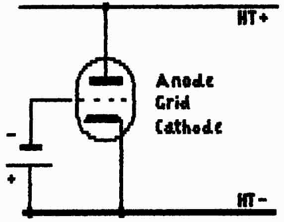
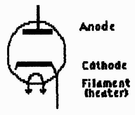
The simplest valve is the diode; the name derives from the prefix di meaning two. As illustrated in Fig.1 it has two electrodes within an evacuated envelope. One of the these, the cathode, is specially treated so that, when heated, if gives off a cloud of free electrons. These form a space charge around the cathode within the evacuated envelope. In early valves the cathode was a simple heated filament similar to an electric lamp but so-called indirectly-heated valves now use a cylindrical cathode with a filament heater mounted inside it. You may encounter a valve in which he cathode is simply a filament where that valve is intended for low-voltage working in small dry-battery-operated equipments. |
>>>>>>>>>>>>>>>>>>>> PAGE 11 <<<<<<<<<<<<<<<<<<<<
The second electrode or anode is a metal plate which surrounds the cathode. When charged negatively with respect to the cathode it repels the space-charge back toward the cathode. When charged positively with respect to the cathode it attracts the electrons of the space-charge and so a flow of electrons (an electric current) occurs from the cathode to the anode.
As described in Part-2 (Detectors) and in Part-5 (Rectifiers) such "one-way" diodes can be used to convert ac supplies to dc.
Triode valves, as the name implies, have a third electrode and this takes the form of a metal mesh or a spiral winding mounted between the cathode and anode. In all valves except the diode the anode is always maintained at a positive potential (with respect to the cathode) so that anode current flows continuously. When the grid is made negative with respect to (w.r.t.) the cathode then it repels electrons back toward the cathode and so reduces the anode current. Over a range of grid-cathode (negative) voltages the change of anode current is reasonably proportional to the change of grid voltage - we say that they are linearly related.
|
When the grid is made positive w.r.t. the cathode it accelerates the electrons and so increases the anode current BUT it also collects some of those electrons causing a flow of grid current; as a result the increase in anode current does not accurately reflect the increase in grid voltage. Except for Class-C operation the grid is not allowed to draw current because of the ensuing distortion and also because few valves can withstand the heat generated at the grid. As long as the grid is maintained negative w.r.t. the cathode the input (grid-cathode) is open-circuited and so only the voltage waveform is of importance. Fig. 3 shows the basic action of a valve as a voltage-amplifier. |
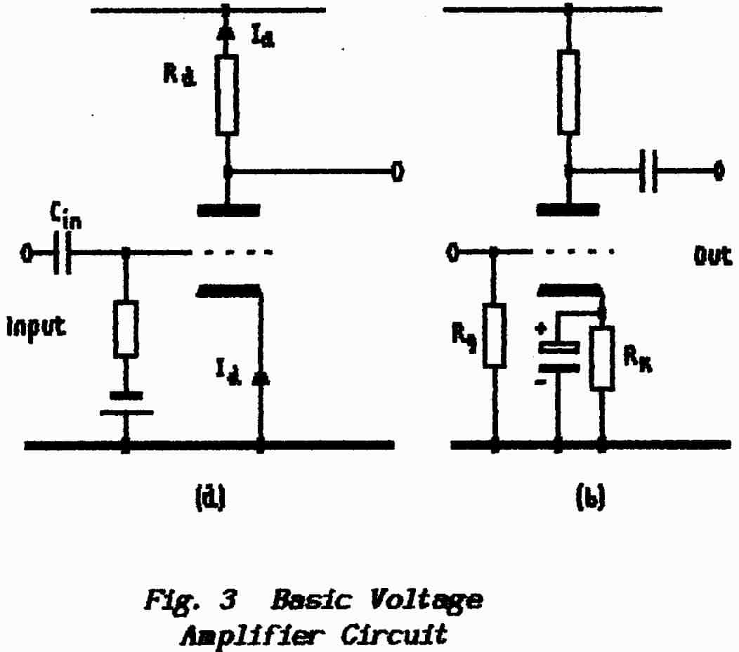 |
The anode current (Ia) is
drawn from the auxiliary supplier (the high-tension or H.T. source) through an anode-load resistor Ra (Note - this is a capital R) and, as a consequence, there is a p.d. across the resistor given by Ohm's Law as Ia x Ra Because of this p.d. the anode potential is less than that produced by the auxiliary source. At any moment in time the anode-current, and consequently the anode potential, is determined by the voltage on the grid w.r.t. the cathode. |
>>>>>>>>>>>>>>>>>>>> PAGE 12 <<<<<<<<<<<<<<<<<<<<
Without a signal input the value of Ia is determined by a standing bias-voltage on the grid which is set so that the anode potential is about half-way between the H.T. value and ground. An alternating signal-voltage applied to the grid, and mixed with the bias, thus causes the anode potential to rise and fall in sympathy with the grid-input voltage. A simple circuit of this nature is shown in diagram (a). The capacitor Cin isolates the signal source from the bias.
Diagram (b) shows the usual arrangement. The biasing requirement is that the grid should be negative w.r.t. the cathode. This is equally served by making the cathode positive w.r.t. the grid. Bias for the cathode can be developed by inserting a cathode-bias resistor (Rk) between cathode and ground line. The anode-current must flow through this resistor to return to the cathode and, in doing so, it raises the cathode positive w.r.t. that ground line by a p.d. equal to I x Rk.
At this stage we are interested only in developing a cathode bias; i.e. a direct potential. With an alternating signal present at the grid the bias across Rk must vary in sympathy with the signal waveform. This is avoided by connecting a large-value capacitor Ck across the cathode-resistor as shown. This capacitor is an electrolytic capacitor which must be connected correctly ; note the symbol. There are two ways of considering the action of Ck:
(a) the cathode-bypass capacitor must have an impedance to the ac which is much lower than Rk; as a result the alternating component of the current flows only through the capacitor while the direct component flows only through the resistor
(b) the time-constant of Ck.Rk (see Funds-1, Lesson-3) must be large enough that the cathode-capacitor cannot charge (or discharge) in the time permitted by each cycle of the signal waveform.
The grid has a tendency to intercept electrons as they pass through and, as these accumulate, so they produce a negative potential on the grid. A grid leak resistor Rg is necessary to return these electrons to the cathode,
Tetrode and pentode valves are made which have respectively two and three grids. The second grid (the screen-grid) is held at a constant positive voltage, as indicated in the manufacturers' data, by means of a dropping-resistor; this functions in the same way as the cathode resistor and needs to be decoupled with a large-value screen-decoupling capacitor. This screen grid reduces the internal stray capacitances of the valve (a Faraday Screen) and also enables it to produce higher voltage-gain.
The third suppressor grid is connected either to the cathode or to ground; its main function is to prevent a "negative-resistance" effect caused by electrons ejected from an overheating anode flowing to the screen grid. (The result is that the anode current falls as the anode voltage is raised.)
Valves circuits are not examined for the R.A.E. except for transmitter valve-operated P.A. stages
>>>>>>>>>>>>>>>>>>>> PAGE 13 <<<<<<<<<<<<<<<<<<<<
As with valve devices the simplest semiconductor
device is the diode. These come in many different constructions but the basic
operation is as follows. A semiconducting material is doped at one end as n-type
and at the other end as p-type; see Fig.4.
This means that one end of the material is rich in electrons and the other
end is rich in holes. This is known as a p-n Junction.
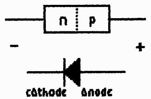
Fig.4 Forward-biased P-N Junction Diode |
Such a construction results in the formation of a potential "barrier" at the junction of the two types and the electrons and holes are driven away from this. When a p.d. is applied across the ends of this device, such that the n-type is made more positive than the p-type, the tendency to migrate toward the ends is encouraged; because electrons and holes may not come into contact it is not possible for an electron current to flow. |
When the n-type material is made more negative than the p-type material, as shown in Fig.4 , electrons are repelled toward the p-type and drawn across the barrier toward the more positive potential and so an electron-current flows from negative-to-positive. This is equivalent to a flow of classical-currrent from positive-to-negative (i.e. from p-type to n-type material).
The two most common types of diode are made from Germanium and Silicon. Germanium-based diodes offer forward conduction voltages around 0.2-volt and are ideal for small-signal applications such as detectors. However they are not very robust in terms of voltage and power-dissipation. Silicon diodes offer forward-conduction voltages around 0.6-volt which is less efficient for very-small signal rectification but they can handle relatively large powers because of their ability to withstand higher temperatures.
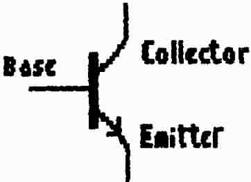
The simplest transistors have three connections and may be likened to the triode valve. The earliest were the bipolar transistors which get their name because conduction takes place through the agency of both majority and minority carriers (see Lesson-1 in Fundamentals-1).
Fig.5 Bipolar Transistor |
As shown in Fig.5, current from the auxiliary supplier flows through these transistors between an emitter and a collector and its value is determined by the current injected between the emitter and a base connection. The signal-current which flows between collector and emitter is greater than the input signal-current by a factor known as the current-gain and given the symbol hFE. |
An improved transistor for many purposes is the Field-effect transistor or FET which has an open-circuited input in much the same manner as does a valve. Indeed, except for the lower direct potentials required, it can often be used in exactly the same manner as a valve.
>>>>>>>>>>>>>>>>>>>> PAGE 14 <<<<<<<<<<<<<<<<<<<<
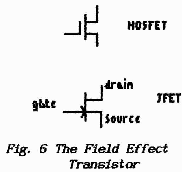 |
In a FET the input connection is a gate which is the equivalent of the base in a bipolar transistor or of the grid in a valve (the analogy should not be taken too literally) ; see Fig.6. The gate is insulated from the main structure (the substrate) . The current from the auxiliary supplier flows from a source to a drain and passes between the gate and substrate (body of the device). An appropriate voltage applied between gate and substrate "pinches-off" this current thus acting as a current regulator. |
END OF LESSON 2
* * * * * * *
QUESTIONS
1. Why is a differential-amplifier useful as a measurement tool ?
2. Briefly what is a modern Op-amp ?
3. Give the main differences between valve-operated circuits and transistor circuits.
4. Why does a valve need a filament supply ?
5. What is the function of the grid in a triode valve ?
6. Re-draw Fig. 3(b) using a bipolar transistor.
7. The emitter-bias resistor has a value of 1 k-ohms. Give a suitable value for the bypass capacitor if the stage has to handle a signal of 100 Hz.
>>>>>>>>>>>>>>>>>>>> PAGE 15 <<<<<<<<<<<<<<<<<<<<
** The basic amplifying device has three connections ; current from the auxiliary power-supplier flows between two of these under the control of an input-signal which is applied to the third.
In the vast majority of circuits one of these electrodes is either earthed or it is maintained at earth potential for alternating signals. This is convenient in terms of safety, the elimination of noise signals and the control of stray couplings.
Fig. 7 shows the basic arrangement in what appears to be two forms. In diagram (a) the signal source is returned to the lower of the two other electrodes and, in diagram (b), it is returned to the upper of the two electrodes. In terms of signal currents the two forms are in fact identical.
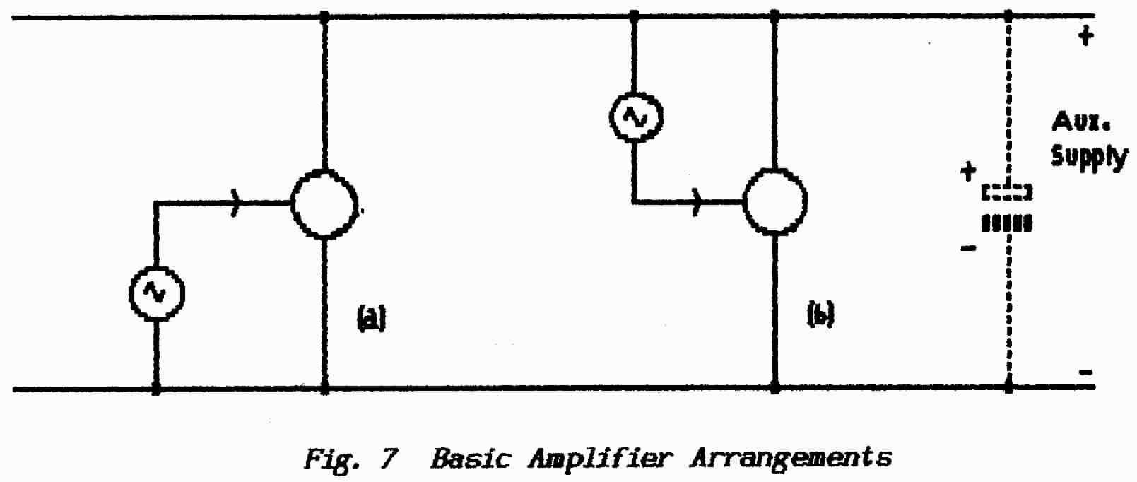
** The auxiliary supplier is required to provide dc and so it contains large-value smoothing capacitors which are connected directly between the two supply lines ; see Part-5. The low-impedance of these ensures that alternating potentials cannot develop across the dc supply thus, as far as ac-signals are concerned, the two supply lines (one positive and the other negative) are connected together.
** Where equipment is operated from batteries it is usually necessary to connect a "by-pass capacitor" across the supply lines to ensure that there is a low-impedance path around the battery for signal currents. Without this the battery acts as an impedance which is common to all amplifier stages and the resulting inter-stage coupling can result in a low-frequency oscillation known as "motor-boating"
Provided that the dc-supplier is properly decoupled the input signal-source may be returned to either line as may be necessary to suit dc-requirements. Precautions are necessary of course to ensure that the signal-source does not draw direct-current from the supplier.
Note that an Earth connection is not shown in either of these two diagrams because it is not relevant to the action of the circuit. This earth can be connected wherever it is most convenient and this gives rise to three possibilities:
>>>>>>>>>>>>>>>>>>>> PAGE 16 <<<<<<<<<<<<<<<<<<<
** Fig. 8 shows the basic configuration with the collector connected directly to the supply line ; as explained above this is exactly the same signal-wise as connecting the collector to the grounded side of the supply. The signal current injected between base and emitter controls the flow of collector-emitter current.
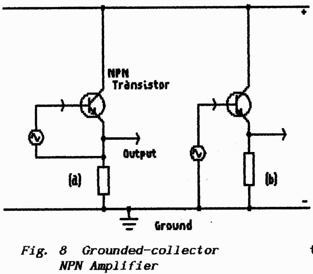 |
** It is convenient here to introduce one of the complications of semiconductor devices which arises from their construction using both p-type and n-type materials (see Lesson-1 of Fundamentals-1). ** Bipolar transistors are built as sandwiches of p-type and n-type material and, according to the structure, are known as either pnp or npn transistors. For the R.A.E. the only significant detail is that pnp transistors require a negative supply-line while npn types require a positive supply-line. The difference is shown in circuit diagrams by the direction of the small arrowhead which delineates the emitter (the collector is not marked). An outward-pointing arrow indicates an npn transistor. |
** Diagram (a) shows the input-signal connected between base and emitter and this is simply the basic diagram of Fig. 6 with the earth connection taken to the collector. A load resistor is connected between the emitter and ground so that the collector-emitter current develops an output-voltage.
** A more convenient, and more usual, connection for the driving source is shown in diagram (b) where the source is returned to ground rather than to the emitter (if you prefer it the signal-source has now been returned to the collector). As a result the input circuit between base and emitter now contains the output-voltage in series with the source-voltage. This is an example of negative-feedback in which ALL the output voltage is fed back to the input and it has two important consequences:
(i) If (say) the base is taken more positive with respect to the emitter then the collector-emitter current increases, the p.d. across the emitter resistor increases and so the emitter too goes more positive. For this reason the arrangement is referred to as an emitter-follower circuit. Whatever happens to the base is imitated by the emitter.
>>>>>>>>>>>>>>>>>>>> PAGE 17 <<<<<<<<<<<<<<<<<<<<
(ii) For the base-bias to remain positive w.r.t. the emitter the voltage-excursion at the emitter must be smaller than the excursion at the base. This means that the signal-gain, from input to output, must be less than 1 - there is always a slight voltage-loss.
** This may appear to be a poor amplifier and, in terms of voltage gain, so it is. The analysis of the circuit is not required for the R.A.E. and it is necessary to note only that the circuit provides a high input impedance and a very-low output impedance ; in other words it is a current-amplifier. It is a most useful device for driving low-impedance or capacitive (frequency-conscious) loads where it is required to buffer (i.e. to protect) the circuit from the effects of any load. Note that the output voltage is in phase with the input voltage ; i.e. if the input signal goes positive then the output also goes positive.
Where the circuit is built using a valve it is called a cathode-fol1ower.
** Fig. 9 again shows the basic amplifier circuit but this time it uses a valve with the input-connection (the grid) connected to ground. The flow of anode-cathode current is controlled by the voltage which is impressed between the grid and cathode connections thus, if the grid is to be earthed, the stage must be driven by varying the voltage of the cathode.
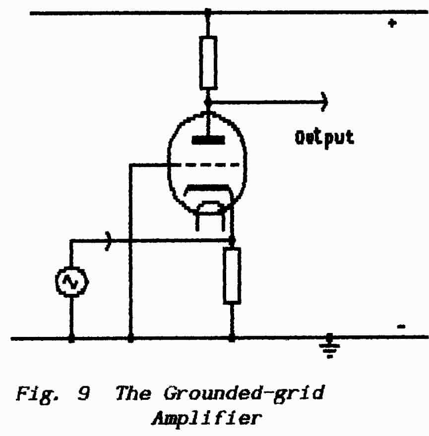 |
** The circuit has much in common with the cathode-follower
described above except that this time only part of the output-voltage is
developed across the cathode resistor ; a much larger output voltage
appears across the anode load. The source and fed-back voltages are now
in parallel. The great advantage of this arrangement is that the
earthed grid acts as a Faraday Screen between anode and cathode and
so eliminates the effect of the anode-grid capacitance. In rf-amplifiers
this capacitance can provide unwanted positive-feedback..
If, say, the cathode is driven positive then the grid becomes more negative w.r.t. the cathode and so the valve draws less current. Less anode-current means that the voltage developed across the anode-load resistance is decreased and so the anode potential moves toward the positive supply line. Thus once again the input and output voltages are in phase. |
>>>>>>>>>>>>>>>>>>>> PAGE 18 <<<<<<<<<<<<<<<<<<<<
** This version of the basic circuit, shown in Fig. 10, is the most frequently occurring form. In this it is the emitter which is earthed.
** However, there are a few extra complications which arise from the deficiencies of the bipolar transistor. These transistors suffer from leakage current which flows from the collector to the base and this current drives the transistor into conduction. The resulting power-dissipation causes the device to generate heat which further increases the leakage-current. The result is a phenomenon known as thermal-runaway which quickly destroys the transistor
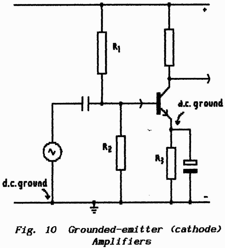 |
** The cure for this problem is dc negative-feedback
and this is the purpose of the two resistors in the base circuit and the
third resistor in the emitter circuit which are designated R1,
R2 and R3. The base-resistors form a potential-divider
across the supply ; they have relatively low-values so that they form a
constant-voltage source to which the base is connected. If (say)
the collector-emitter current tends to increase this causes an increase
in the p.d. developed across R3 and this, by raising the potential of the
emitter (against the constant potential of the base), reduces the base-emitter
voltage and so tends to oppose the increase of collector-emitter current.
** A large-value electrolytic capacitor is also connected between emitter and ground to provide a low-impedance path for the ac signal-component; this prevents a signal voltage developing across R3 which, as ac negative-feedback, would reduce the overall stage-gain. |
In a valve version of this amplifier, and also in the FET version described below, the cathode-resistor Rk serves to generate automatic bias for the amplifier. As described earlier this sets the correct operating point for the valve by raising the cathode-voltage with respect to the grid. Thermal runaway is not a problem because valves do not suffer from leakage currents and so the low-impedance potential-divider circuit is unnecessary. However a grid leak resistor is required as described above to ensure that the grid does not become negatively-charged.
It is not unusual to see circuit diagrams in which the envelopes of valves or transistors are omitted; in practical situations the omission is a matter of convenience and speed but there is not a rule.
>>>>>>>>>>>>>>>>>>>> PAGE 19 <<<<<<<<<<<<<<<<<<<<
** The field-effect transistor (FET) is a transistor which uses a different method of current-control as described in Lesson-2 of this Part. The emitter and collector of the bipolar transistor are replaced by a source and a drain between which current flows in a channel . The effective "size" of this channel is controlled by an electric field which is set-up by applying a voltage to a gate (which replaces the base of a bipolar transistor).
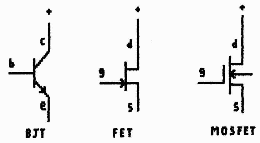
Fig.11 Comparison of Bipolar Transistor and FET |
** The great difference between these two types
of transistors is that a gate electrode is insulated from the main structure
and therefore it does not draw current. Only the electric field is concerned
and so the passage of auxiliary current between source and drain is determined
by the voltage applied to the gate. Thus an FET
is, in effect, a solid-state valve.
Note that the gate symbol indicates which connection is the source. It indicates also whether the channel material is p-type or n-type by means of the small arrow and it is here that complications begin to accumulate.
|
The FET device shown in Fig. 11 has an inwards-pointing arrow which indicates an n-channel and thereby that the device requires a positive supply. Alas ; thereafter it gets ever more confusing but, fortunately, you are not required to sort them out for the R.A.E.
** FET devices come with two kinds of gate construction:
1. semiconductor junction (JFET)
2. metal-oxide-semiconductor insulated (MOSFET) sometimes known as insulated-gate FETs or IGFETs.
In the first kind the gate electrode is formed as a PN-diode junction exactly as in the bipolar types ; as a result, if it is allowed to become forward-biased, the gate will draw current.
In MOSFET devices the gate is insulated by a very-thin layer of glass and so it can be biased in either direction without drawing current. When the gate potential is carried toward the supply potential conduction takes place between source and drain.
** The glass insulating-layer is extremely thin and so vulnerable to damage by static charges such as may exist on a human body ; thus, unless precautions are taken to discharge all static, a MOSFET will be destroyed simply by the act of picking it up. However, once soldered into position on a circuit board, the risk is much reduced.
>>>>>>>>>>>>>>>>>>>> PAGE 20 <<<<<<<<<<<<<<<<<<<<
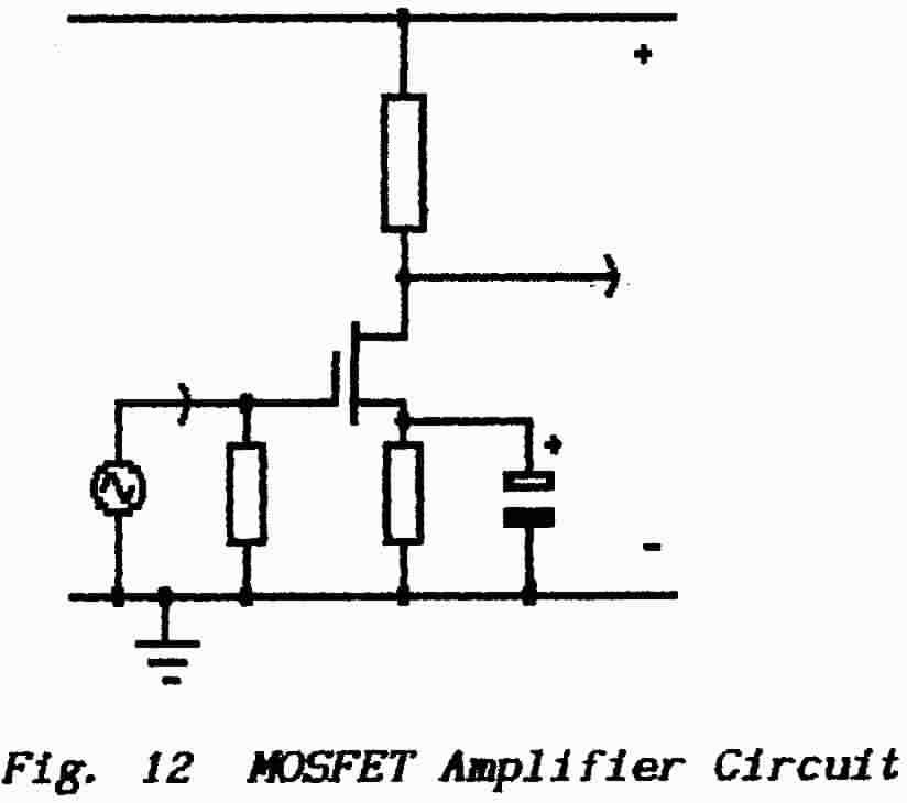 |
** Fig. 12 shows a
basic voltage-amplifier circuit using a MOSFET. Compare this with
the bipolar transistor amplifier in Fig.10.
** In both voltage-amplifier circuits there is a limit to the amplitude of the input signal. At one extremity the transistor or valve becomes completely cut-off, the p.d. across the load becomes zero and so the drain (anode) voltage rises to the value of the positive-supply line. The output cannot rise beyond this value. ** At the other extremity the device is driven heavily into conduction with the result that the p.d. developed across the load drives the drain (anode) voltage to a minimum value. For a valve this is around 50 volts but for a silicon transistor it is around 0.6 volts. In this condition the device is said to be saturated or bottomed. |
** For the output signal to be a faithfull.copy of the input waveform there needs to be a linear relation between input voltage and source-drain current (cathode-anode current). Such a relation only holds however over a limited part of the excursion from cut-off to saturation ; to amplify the positive half-cycles and negative half-cycles equally it is necessary to ensure that:
(i) the zero-level of the input signal coincides with the centre of the linear range ; this is the purpose of the bias voltage that is developed across the source (cathode)resistor.
(ii) the amplitude of the input signal does not exceed the linear part of the range
This is a Class-A amplifier circuit.
** The simplest method of applying feedback to an amplifier stage is to omit the bypass capacitor which normally is connected across the source (cathode) resistor. The varying dc which flows through the resistor now generates a varying direct-voltage instead of the steady direct-voltage which is required for biasing. Note that this feedback voltage is developed from the output-signal current and so represents a sample of the output current. One effect of this arrangement therefore must be to stabilise the output current ; i.e. it raises the output (or source) impedance of the amplifier stage.
This feedback voltage appears in series with the input voltage between gate (base or grid) and source (emitter or cathode) and so tends to cancel the input-signal voltage . The result is to reduce the stage-gain but it can be expressed as a need to raise the input voltage to maintain the same level of output voltage.
>>>>>>>>>>>>>>>>>>>> PAGE 21 <<<<<<<<<<<<<<<<<<<<
The need to raise the voltage implies that the input-impedance of the stage has been increased.
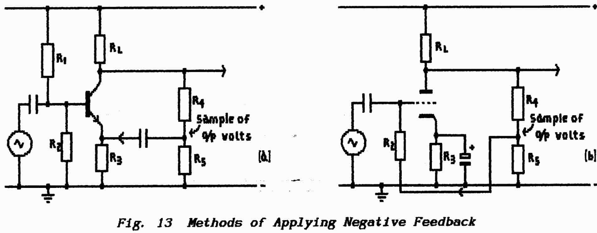
** Fig.13 shows two methods of applying voltage-derived feedback. These arrangements, because they sample the output voltage, tend to stabilise that output voltage which implies that the output impedance has been reduced.
In diagram (a), where the feedback voltage is applied to the emitter, then the input impedance is again increased. In diagram (b), where the feedback voltage is applied to the grid, the input and feedback signals appear at the grid in parallel. When (say) the input-signal source is trying to supply current so the negative-feedback source is abstracting current and so the source experiences a demand for more current ; it interprets this as a reduced input impedance.
(For the R.A.E. feedback circuit arrangements are not examined in great detail. Familiarise yourself with this Section but do not put too much emphasis on trying to learn it.)
In connection with the cathode by-pass capacitor (emitter by-pass capacitor) shown in the above diagrams the reactance of the component increases as the frequency is decreased. Thus, at low frequencies, the component fails in its task of decoupling and the circuit gain falls as negative-feedback develops.
Although not generally regarded as a feedback-amplifier arrangement nevertheless the process of neutralising rf-amplifiers does use feedback techniques.
A problem arises from the natural (stray) capacitance which exists between the anode and grid of a valve (or the similar electrodes of semiconductor devices) and the natural stray capacitances which exist between parts of the input and output circuit components. At radio frequencies such small-value strays offer a low-impedance path to signal currents and so part of the output signal from an amplifier stage is fed back to its input circuit.
>>>>>>>>>>>>>>>>>>>> PAGE 22 <<<<<<<<<<<<<<<<<<<<
Depending on the tuning of the various circuits these inherent feedback paths may result in either negative-feedback or positive-feedback or a variety of conditions between the two extremes. The result is either an uncontrollable oscillation or obscure forms of misbehaviour from the would- be amplifier stage.
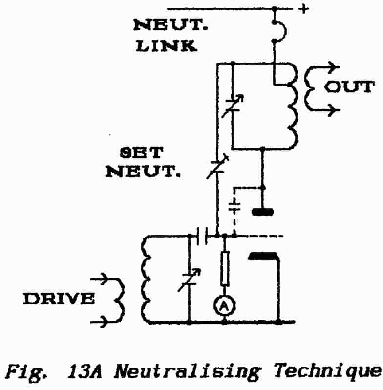 |
The strays themselves can be reduced by careful design but they cannot be eliminated and so circuit designers have dreamed up a variety of tricks to eliminate their unwanted effects . Fig. 13A illustrates the basic idea in which a small sample of the output signal is derived with "opposite phase" (i.e. 1800 phase shift) and this is fed back also to the input circuit. The trick lies in adjusting the level of this fed-back signal so that it exactly cancels (neutralises) the unwanted signal. |
One technique is to disable the stage (by disconnecting the dc power-supply) and, with the rf-drive in operation, the output-circuit tuning is then varied. As the output circuit passes through resonance at the drive frequency so it absorbs power from the drive via the stray coupling ; the consequent load imposed on the drive-source causes a fall in its output level and this is reflected by a fall (a dip) in the input current. The level of the neutralising-signal is adjusted until this dip is minimised thus showing that cancellation is taking place.
END OF LESSON 3
* * * * * * * * * * * * * *
QUESTIONS
1. From the signal point of view why is it that the source may be connected either between the input and earth or between the input and supply line of an amplifier ?
2. Why do we use emitter-followers with their voltage-loss ?
3. What is the main objective of a grounded-grid amplifier ?
4. Why is a large-value capacitor connected between emitter (or cathode) and ground in a grounded-emitter amplifier ?
5. What is the advantage of using a FET transistor against a bipolar type?
>>>>>>>>>>>>>>>>>>>> PAGE 22 (again) < <<< < <<<<<<<<<<<<<<<
The audio amplifier is often considered to be a simple straightforward arrangement because it handles low frequencies. In fact it has a very-large relative bandwidth covering some eight octaves.
The design of a high-quality audio amplifier can be a tricky business. I have lost two workshop loudspeakers because a "hi-fi" amplifier of considerable power intermittently burst into a supersonic (above audible range) oscillation. Any audio amplifier with a hissy background noise should be checked for performance as an rf-oscillator but even this is complicated by today's habit of designing power-suppliers without smoothing chokes. The resulting large current-peaks drawn from the mains often make an otherwise well-behaved amplifier sound as though it were oscillating.
** The R.A.E. is not concerned with high-quality reproduction of sound but only with the audio stages of receivers. There is however a requirement for good design in microphone circuits, modulator circuits and auxiliary circuits such as speech processors.
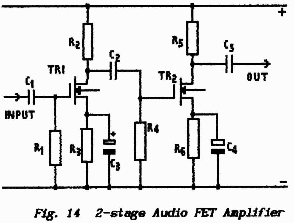 |
** A basic single-stage audio amplifier circuit is shown in Fig.12 of the previous Lesson and is reproduced again here as a 2-stage amplifier (Fig. 14). The FET device shown can be directly replaced with a valve provided of course that suitable adjustments are made to the supply voltages and component values. ** The object of a 2-stage amplifier is to increase the overall gain but cascading two stages in this manner introduces a few complications.
|
** The signal applied to the gate of the second stage is much larger than the non-amplified signal applied to the first stage and so it may be necessary to use a different bias for the second stage by changing the value of the source-resistor R6. A change of bias means that the standing current (the current without signal input) is changed and so it may be necessary to adjust the drain-resistor R5 also. It may also prove necessary to use a transistor of different signal-handling capability in the second stage.
** The coupling capacitorC2 must be introduced to ensure that the direct-potential at the drain of transistor TR1 does not bias the gate of transistor TR2. The resistor R4 must then be introduced as a leak to ensure that C2 does not acquire a charge which again would bias the gate of TR2. The combination C2 and R4 is known as an RC-coupling.
** An RC-coupling introduces a new complication in that it is frequency-conscious. At low frequencies the reactance of the capacitor increases and a proportion of the (alternating) signal voltage appears across it so reducing the amplitude of the signal applied to TR2.
>>>>>>>>>>>>>>>>>>>> PAGE 23 <<<<<<<<<<<<<<<<<<<<
Source decoupling-capacitors suffer the same frequency-related problem and so again, as frequency falls, the steady bias turns into bias+signal. The resulting negative-feedback reduces the stage gain at low frequencies.
To reduce the effects of small distortions negative feedback may be applied either overall, to the individual stages or in both arrangements simultaneously. As already mentioned in earlier Lessons the rule is that n.f.b. can be used to improve a good amplifier - but not to make a bad design work. The frequency dependent attenuation introduced by circuit components such as RC-couplings and bypass capacitors is accompanied by phase-shifts and, if these become too large, the n.f.b. is converted to p.f.b. As a result the amplifier develops bad habits of which perhaps the most obvious is a continuous oscillation. Depending on the severity of the phase-shift, and the amount of gain available, an amplifier may burst into oscillation only on the positive peaks of a signal waveform.
Excessive phase-shifts occur in multi-stage amplifiers because the effects of RC-circuits are additive. A simple cure for this is to arrange that all the RC combinations have different time-constants(the product of resistance and capacitance) which ensures that phase-shift effects from each combination do not overlap.
** Audio amplifiers which provide either voltage or current gain invariably operate in Class-A while output (power) stages may be found in Class-A, Class-AB or Class-B . As discussed in previous Lessons power amplifiers in any mode other than Class-A must be push-pull arrangements and would normally incorporate n.f.b. loops to reduce the last traces of distortion. Such distortions are particularly noticeable at zero crossover points where the two halves of the waveform are assembled.
** A Class-A 2-stage circuit using bipolar transistors is shown in Fig.15 and it differs from the FET circuit of Fig.14 in one important way. The FET is voltage-operated and would therefore be used to amplify a voltage waveform. Thus the value of each drain resistor would be adjusted so that, without an input signal, the drain potential lies midway between that of the supply line and the bottoming voltage of the transistor.
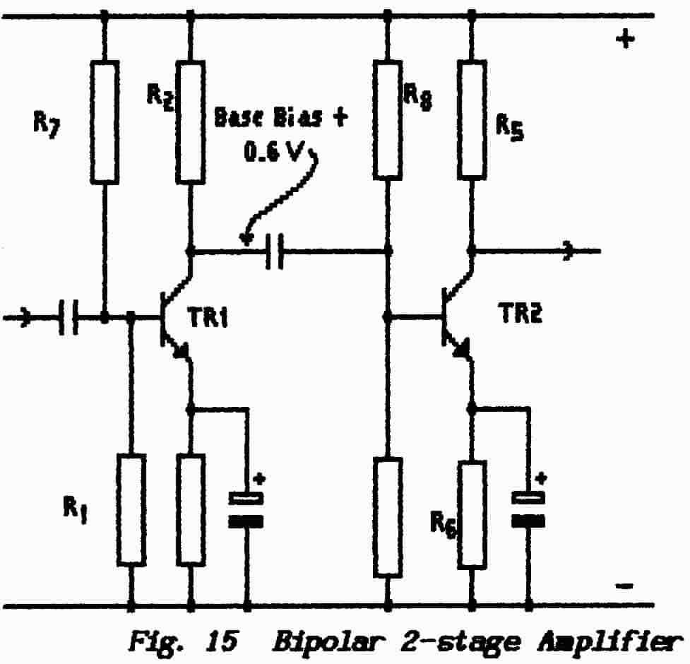 |
** The bipolar transistors are current operated. To provide amplification it must be arranged that, when TR1 demands an increase in collector current, the extra current is drawn from the base of TR2. Similarly, when TR1 demands less collector current, the surplus current is passed to the base of TR2. To this end the value of TRI collector-resistor is chosen so that, without input signal, transistor TRI is bottomed. The resistor cannot pass more current and so any extra must be drawn from the base of TR2; when TRI collector-current decreases then the collector-potential tries to rise which increases the base-current of TR2. |
>>>>>>>>>>>>>>>>>>>> PAGE 24 <<<<<<<<<<<<<<<<<<<<
A proper understanding of this is important when fault finding. An oscilloscope (which is voltage-operated) attached to the drain of Tr1 in Fig.14 would display the amplified signal-voltage waveform. An oscilloscope attached to the collector of TR1 in Fig.15would show a puzzling small-amplitude voltage waveform with considerable distortion.
The value of the resistor in TR2 collector depends on the nature of the following stage. If it is to drive a third amplifier then TR2 would be bottomed also when in the quiescent state. If the output is required as a voltage then TR2 collector-potential is set midway between the supply line and the bottomed potential.
** It is possible to use a transformer coupling either between stages or as an output-coupling device. For the FET circuit (arid also for a valve circuit) this would be a step-up transformer from drain to high-impedance gate thus providing additional voltage-gain. For the bipolar arrangement it would need to be a step-down transformer from collector to low-impedance base thus providing additional current-gain.
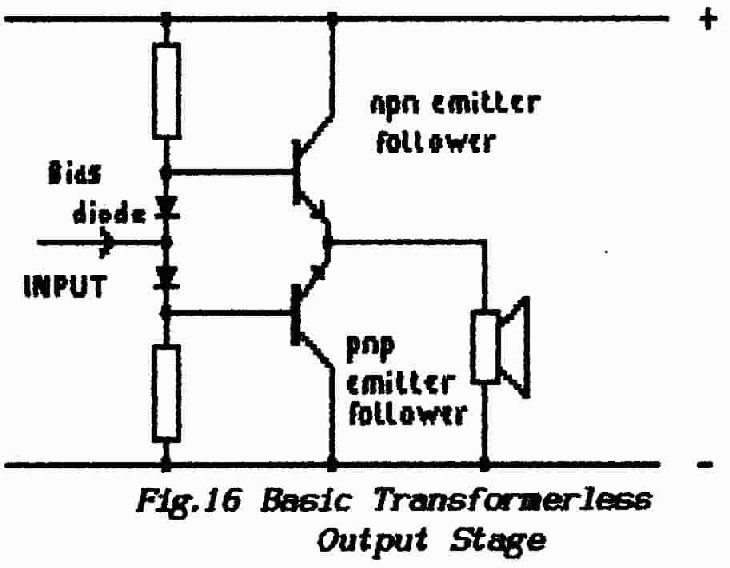
** In single-ended power amplifiers (not push-pull) a transformer coupling is essential between the final output stage and a loudspeaker but push-pull arrangements permit one of the so-called transformerless circuits.
|
** A basic form of this is illustrated in Fig.16 With transistors such a circuit can be designed to provide an output-impedance at the centre point which is suitable for the direct connection of a loudspeaker. There are a variety of practical circuits each of which seeks to overcome one or more of the problems inherent in the transformerless design. The circuit is not examined for the R.A.E. but details are to be found in the literature. |
** Note that, with an inductive load, the quiescent voltage(without an input signal) at the collector (or drain) is that of the supply line because of the low-resistance of the transformer primary winding. Passage of the alternating signal current induces signal voltage across the primary winding and so the collector voltage swings both above and below the supply-potential. The sum of the supply voltage and peak signal-voltage must not exceed the maximum rated voltage of the transistor and a diode catching circuit may be included to ensure that the maximum voltage rating of the device is not exceeded.
** The description RF-amplifier is a little loose in that it covers several different types of amplifier although all are used to amplify radio-frequency signals ; i.e. frequencies above the audio range. They include:
(a) the "front-end" stages of receivers either the pre-detector stages of a TRF receiver or those which precede the frequency-changer in a superhet receiver
>>>>>>>>>>>>>>>>>>>> PAGE 25 <<<<<<<<<<<<<<<<<<<<
(b) amplifier, buffer and multiplier stases in v.f.o., crystal oscillator and synthesiser circuits
(c) the various amplifier stages in transmitters and signal-generators which handle rf signals, whether cw or modulated, including the final P.A. stage and its power drivers and any external Linear Amplifiers which are interposed between a transmitter and the aerial.
Strictly the term applies also to IF amplifiers in that they handle radio-frequency signals. In general it can be assumed that the term rf-amplifier refers to a (variable) single-tuned stage or stages and that if-amplifier is used for the fixed-frequency band-pass stage or stages that follow a frequency-changer.
** A radio-frequency amplifier uses tuned circuits as impedances (compare this with the resistors used in af-amplifiers) because
(i) they provide the narrow bandwidth required for a selective amplifier
(ii) unless the circuits are resonated the stage gain would be destroyed by the low reactances presented by stray capacitances at radio frequencies ; the strays are incorporated in the tuning capacitance thus making use of capacitance that, otherwise, would be a disastrous nuisance
(iii) tuned circuits provide high (dynamic) impedances to maintain stage-gain; if resistive loads were used they would have to be of low value to prevent them being bypassed by stray capacitances.
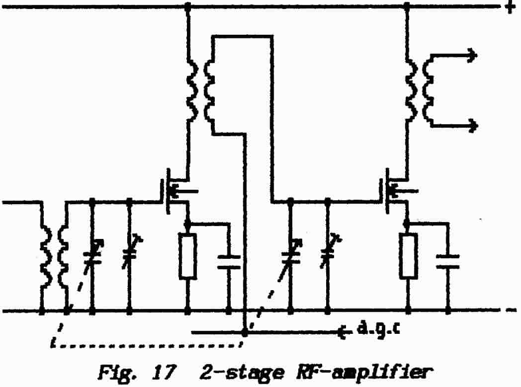 |
** A 2-stage rf-amplifier circuit is shown in Fig.
17. The tuned circuits make couplings easy because
the coils can be constructed as transformers.
** It is necessary to tune each set of coils simultaneously if variable tuning is to be used. It is usual to do this with ganged capacitors so that all tuning adjustments are carried out with a single knob. These are variable capacitors mounted on a common frame with their adjustable vanes mounted on a common (earthed) shaft.
|
** Accurate tuning with such an arrangement however requires accurately- matched inductors and it is easier (and cheaper) to arrange extra variable capacitance known as trimmers; these are shown in Fig. 17 with a hammer-head arrow which indicates that they are variable but pre-set and then left. The tuning capacitors are indicated by the arrows drawn through them and the dotted line which joins the arrows indicates that they are ganged on a single shaft.
Strictly of course trimmers are not required on all stages but the capacitors are manufactured in standard form with the trimmers built-in.
At frequencies above about 100 MHz variable-tuned circuits as described become difficult to handle because of the decreasing sizes of the inductors and capacitors required. As a consequence circuits are encountered which are tuned by:
>>>>>>>>>>>>>>>>>>>> PAGE 26 < <<<<<<<<<<<<<<<<<<<
(a) variable-capacitance diodes whose ganging is adjusted by means of resistive trimmers
(b) variable inductors which are tuned by mechanical adjustment of their ferrite or copper cores (see Lesson 4, Section 1.9.7 in Part 1). Trimming is carried out using small metal vanes which are bent to adjust their capacitance to the chassis and/or by stretching the coils
(c) The tuned circuit may be replaced by a resonant cavity (a metal box) in which it is not at all easy to vary the tuning.
(Circuits of types b & c should not be entered except in dire emergencies and when the necessary test equipment is available.)
** The prime function of a frequency-changer stage in a receiver is to translate the frequency of a signal to that of the IF amplifiers. Nevertheless it is an rf-amplifier and its signal input is variable-tuned. In some receivers the aerial input is taken directly to a frequency-changer stage and so it constitutes the only rf-amplifier in the receiver.
** In a receiver the input (base, gate or grid) of an rf-amplifier is usually connected to the automatic gain-control (a.g.c.) line thus closing the n.f.b-loop that ensures a fairly-constant signal level at the detector. All stages which operate within this loop have fairly-constant signal levels presented to them except when the input-level from the aerial falls below a minimum and the a.g.c. action fails.
The one exception to this rule is the first rf-amplifier, the stage which receives its input directly from the aerial. The problem is that, with a strong incoming signal, the stage is trying to cope with an unusually-large input signal at a time when the e.g.c. voltage is reducing the ability of the stage to handle it. On the other hand this first stage is the most effective point at which a.g.c. can operate. The very first stage of a receiver is often left without a.g.c. or only a portion of the a.g.c. voltage is applied.
The a.g.c. voltage changes not only the gain of a stage but it also modifies the characteristics of the active device. The input and output inter-electrode capacitances of the device form part of the resonant circuits and, when these change value with changing a.g.c., so the resonant circuits become de-tuned. This can be corrected by resorting once again to negative feedback. In valve amplifiers a resistor as small as 10-ohms (un bypassed) in the cathode lead gives sufficient n.f.b. to stabilise the tuning over the full range of input signals. No doubt the same technique works with semiconductor circuits but my experience in this technique is limited to valves.
** With rf-amplifiers it is necessary to provide shielding between input and output circuits of each stage. Although stray capacitances may amount to no more than a few picofarads their reactances at radio frequencies can be sufficiently low to provide good feedback paths and so cause instability. The most obvious cause of this problem can be seen in multi-stage rf-amplifiers where the output and input circuits of a stage are both formed by resonant circuits tuned (nominally) to the same frequency ; in Part 4 such a circuit arrangement is offered as a (tuned-anode-tuned-grid) T.A.T.G. Oscillator.
>>>>>>>>>>>>>>>>>>>> PAGE 27 <<<<<<<<<<<<<<<<<<<<
** The varying voltage on the a.g.c. line causes the standing current in each rf and if stage to vary with the signal strength. This forms the basis of the signal-strength meter or S-meter which is found on the front panel of most commercial receivers or the various forms of tuning-indicator which appear on domestic receivers. In fact, as signal strength increases, so the a.g.c. action causes the standing current to decrease. A meter which indicates an increasing quantity by deflecting to the left is unfamiliar and confusing and so circuit tricks are used to reverse this action. Alternatively a meter can be constructed with a right-hand zero which simply means that it deflects to the left with increasing current.
Occasionally circuits are encountered which use a wide-band rf-amplifier. Generally such terminology indicates an untuned stage which uses a low-value resistor or low-Q choke as the output load. It is essential that this load has a low-impedance otherwise it will be bypassed by stray capacitances and so the stage-gain must be limited perhaps even to a value of 1. Such amplifiers function mostly as buffers or impedance changers.
Linears or linear-amplifiers are rf-amplifiers whose output level is proportional to the input level ; i.e. they do not cause distortion. They are used at the output of a transmitter to raise its power level. As discussed in Lesson-2 of Part-2 a modulated wave must be amplified in linear fashion else other side frequencies and harmonics are generated. The design of a non-distorting Class-A amplifier does not pose many problems but, at the output of a transmitter, there is a requirement for power. The lack of efficiency in a Class-A stage poses a problem in heat dissipation and so Class-B or Class-AB is a more likely choice, The subject is not examined for the R.A.E.
Before leaving the subject of rf-amplifiers mention should be made of the arrangements at the output of a transmitter P.A. stage for feeding the developed rf-power to the aerial. Especially in semiconductor equipments the standard output today is a 50-ohm coaxial connector of some sort which, of course, is intended to house the end of a coaxial aerial-feeder.
Coax however is expensive, relatively lossy and short-lived and a popular feeder used to be the 300-ohm balanced open-wire which brings problems of its own. Unbalanced coax outputs often use a simple RC coupling, especially where power levels are low, but for high-power and balanced circuits a transformer is used.
It is possible to find balanced (push-pull) amplifiers driving an unbalanced feeder or alternatively an unbalanced amplifier driving a balanced feeder and it is necessary to find some means of isolating the circuits if the balance is to be preserved. In Fundamentals-1 Lesson-4 mention was made of the Faraday screen which provides electrical isolation while permitting magnetic coupling. In a P.A. stage such a screen takes the form of an earthed wire-grid placed between the primary and secondary windings of the output (air-cored) transformer. (In a.f. amplifiers it takes the form of a non-closed turn of copper foil wound over the inner winding before the outer winding is added.)
>>>>>>>>>>>>>>>>>>>> PAGE 28 <<<<<<<<<<<<<<<<<<<<
END OF LESSON 4
* * * * * * *
QUESTIONS
1. Why is good quality sound-amplification required in transmitter circuits ?
2. What is an RC-coupling? Why does it cause distortion ?
3. What is the difference between small-signal amplifiers and large-signal or power amplifiers ?
4. Why arid how is a Class-A amplifier biased ?
5. In what ways do AF and RF amplifiers differ ?
6. Why is screening important in rf-amplifiers ?
>>>>>>>>>>>>>>>>>>>> PAGE 28 (again) <<<<<<<<<<<<<<<<<<<<
Back to Top of PageAs already mentioned an if-amplifier is essentially an rf-amplifier but with a specific purpose. It amplifies equally over a specified band of frequencies the centre frequency of which does not vary. It achieves its bandpass characteristic by using multiple tuned circuits (or other resonators), coupled together, in place of the single variable-tuned circuits found in normal rf-amplifiers. The term "if-amplifier" is used in reference to both a single stage of amplification and to an entire amplifying unit of several if stages.
** Fig. 18 shows three versions of a basic single-stage if amplifier which uses double-tuned rf-transformers as impedances. The stage uses automatic emitter (source or cathode) bias and the input is returned to ground via the dc resistance of the driving coil.
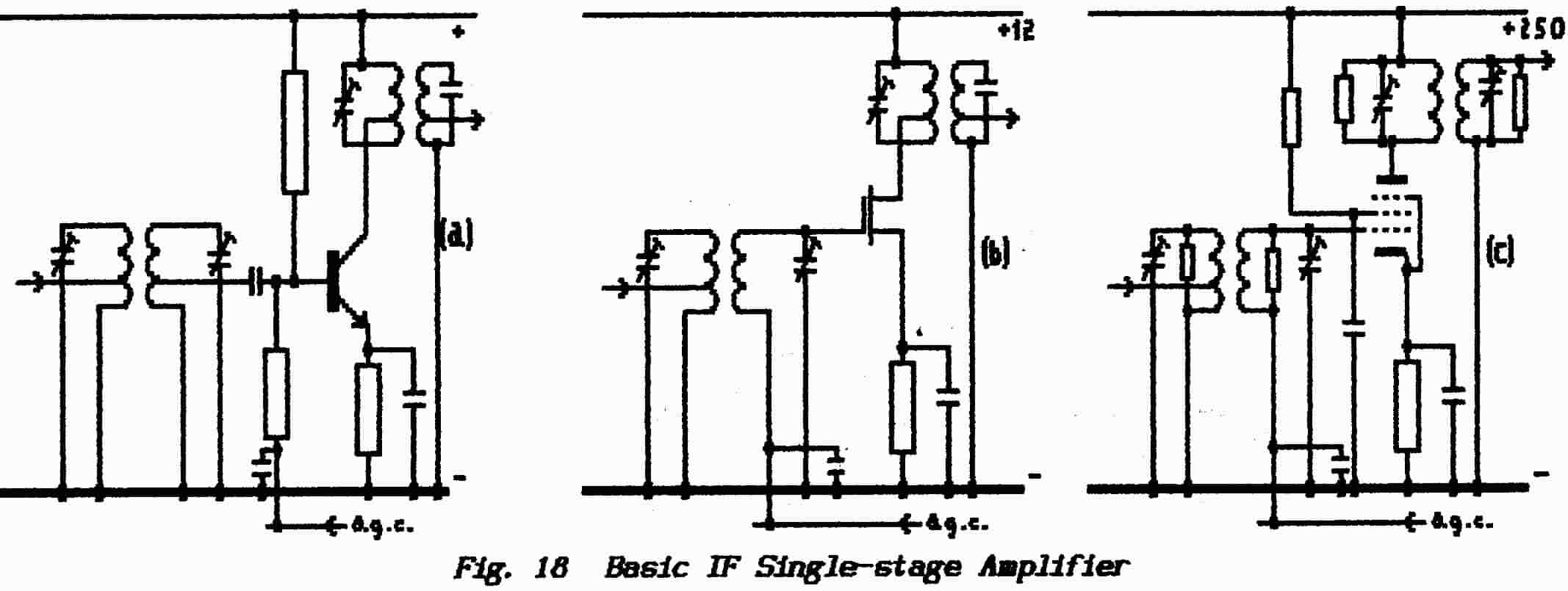
In diagram (a) the bipolar transistor offers a very-low input impedance which would damp the transformer secondary and destroy its Q-value. This is corrected by tapping down the coil which is thus doubling as an autotransformer (see Fundamentals 1, Lesson5). In diagram (b) the FET offers a very-high input impedance and so the tapped coil is not necessary at the gate connection.
Diagram (c) shows the same circuit but using a valve. This too offers a high input-impedance but the valve itself is also a high-impedance device and so the performance is susceptible to the anode-grid capacitance which forms a feedback path between anode and grid. This is overcome by the addition of a screen-grid between the two electrodes which is earthed to signal currents so that it acts as a Faraday screen (see Funds.-1, Lesson-3). Were this screen to be earthed literally it would repel the electron stream which flows from the cathode to the anode ; to maintain the flow of cathode-anode current, the screen is raised to a high potential by connecting it through a dropping resistor to the positive supply line.
The dropping resistor and the decoupling capacitor (which earths the screen-grid to ac-signals) form an RC network ; to prevent a signal-voltage developing on the screen the time-constant RC must be large compared to the period of the signal waveform;
>>>>>>>>>>>>>>>>>>>> PAGE 29 <<<<<<<<<<<<<<<<<<<<
i.e. RC = 5 x 1/f where R is in ohms, C is in Farads and f is in Hertz.
Most small-signal rf valves are fitted also with a third grid making them into pentodes(5 electrodes). The main purpose of this grid is to intercept electrons that may be ejected from the anode ; should these return to the screen the valve may oscillate. This suppressor grid is normally connected directly to the cathode.
** As with rf-amplifiers, the if-amplifiers of a receiver are connected to the a.g.c. line to maintain a constant audio level. However, the final if-stage receives a large signal-input, it must not distort that signal and it is required to supply a certain amount of power to drive the demodulator stage. It is usual either to leave this stage without a.g.c. or to reduce the a.g.c. input.
** For f.m. receivers a.g.c. is not used. The final if-stage is operated as a limiter so that its output drives the demodulator-circuit (the discriminator) with a signal which is free from amplitude modulation. Generally the limiter is driven hard into its limiting mode which action suppresses most of the (a.m.) noise and so provides the high-quality audio signal which is the major asset of f.m. working.
(For those with a flair for such things the limiter produces a bias voltage as part of its action and, provided the if-unit affords sufficient gain, this can be fed-back as an a.g.c. signal.]
The theory of coupled circuits is not required for the R.A.E. A simple explanation is based on the fact that a capacitive reactance at the input of a transformer is coupled into the secondary circuit as an inductive reactance and, similarly, an inductive reactance appears in the secondary as a capacitive reactance.
When the applied frequency is below the resonance frequency both tuned circuits present a capacitive reactance ; thus each circuit reflects an inductive reactance into the other and this tends to preserve the resonant condition. Similarly, when the applied frequency is higher than the resonance frequency, both circuits present an inductive reactance which is reflected as a capacitive reactance into the other.
** To achieve the best result, in which the gain remains constant over the desired band of frequencies, it is necessary to obtain an exact degree of coupling between the two circuits. This particular value is known as critical coupling and its value depends on the inductance of each coil and on the Q of each tuned circuit of the pair.
The initial alignment of such a transformer is reasonably simple. First the two coils are pushed as far apart as possible to minimise the coupling i.e. to ensure that neither detunes the other through reflected reactances. Each circuit is then tuned to resonate at the required centre frequency and the coils slowly pushed together until the required "flat-topped" characteristic is obtained. The coils are then cemented into place.
>>>>>>>>>>>>>>>>>>>> PAGE 30 <<<<<<<<<<<<<<<<<<<<
Sometimes it is not feasible to move the coils (a commercially-supplied unit may have the coils already cemented). Any attempt to resonate the second coil then detunes the first one already set-up. The procedure is to connect a low-value damping resistor across one of the coils thus destroying its Q-value and so rendering it almost non-reactive. The other circuit is then correctly tuned. Next the damping resistor is transferred to the second coil thus reducing its reactive component which enables the remaining circuit to be correctly resonated. Finally the removal of the damping resistor will leave the circuit properly aligned assuming that the coupling was correctly set.
These alignment procedures are not examined for the R.A.E. but the above brief study may help to understand the bandpass arrangement.
The double-tuned transformer is not the only bandpass circuit that can be used but it is the simplest, the cheapest and the most compact. There are occasions however when its compactness can be a problem in that, with the requirement at high frequencies to keep connections short, the designer runs out of room. On such occasions it can be helpful to use two entirely separate coils in separate screening cans and to couple them via a small adjustable capacitor ; this enables the circuit to be spread out without incurring problems with stray inductances.
There is a direct relation between bandwidth, the degree of coupling and the Q of each tuned circuit. Often the active devices do not provide the amount of loss required to achieve a desired bandwidth and so extra loss must be provided In the form of damping resistors. These may be connected across each bandpass coupled circuit either as a single resistor of appropriate value or divided into two separate resistors one of which is connected across each coil of the pair.
There is a purely practical pont here that involves the difficulty of constructing coils/transformers of exactly the required parameters. Under manufacturing conditions where many hundreds of units are to be constructed this can be dealt with but, for a one-off job, it is easier to aim for a too-high Q and add damping resistors on a suck-it-and-see basis.
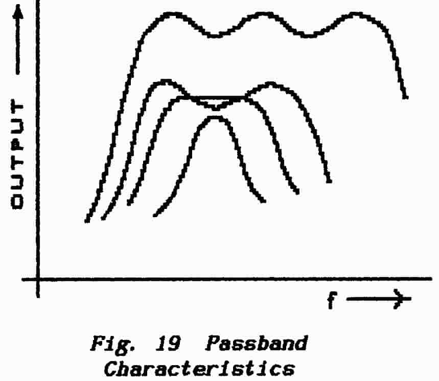 |
Critical-coupling results
in a flat response as shown in Fig. 19. Coupled
circuits are usually adjusted with slightly more than critical coupling
because it gives a slightly increased passband and slightly steeper skirts
at the band-edges. As shown in Fig. 19it
also produces a double-humped characteristic in which the size of the bumps
is easily controlled by adjusting the coupling factor.
Note that a single tuned circuit produces a single-peaked response, a double over-coupled circuit produces two peaks and a triple over-coupled circuit produces three peaks.
|
It is possible to produce bandpass filters which consist of many LC circuits magnetically-coupled as described above; such filters are to be found for example in the Racal RA17 receivers. Unless you have experience in adjusting such circuits and the necessary equipment it is foolish to interfere with these because any alteration to one of the LC combinations detunes all the others. This type of filter is an exact analogy of the Yagi "beam" aerial which consists of a string of resonant rods spaced at critical distances (for distances read coupling-factors). The above discussion of the multi-unit bandpass filter will perhaps make clear why the claims made for Yagi aerials should be taken with a pinch of salt.
>>>>>>>>>>>>>>>>>>>> PAGE 31 <<<<<<<<<<<<<<<<<<<<
The criteria by which such circuits are designed are very simple but not required for the R.A.E. If you have the necessary equipment and wish to construct your own if-unit I will supply the information on request.
Warning Many domestic receivers use stagger-tuned circuits in the if-amplifier section because of the easier alignment. Before attempting to "peak-up" an if. unit make sure that it is using coupled circuits and not stagger-tuning. Adjustment of trimmer capacitors in the latter results in a rapid increase of gain and the onset of self-oscillation as each stage tries its hand as a T.A.T.G. oscillator (see Part 4). A good designer will ensure that, when a coupled circuit is adjusted for critical coupling, the gain per stage is limited to a safe value.
** Communications receivers have a requirement for variable bandwidth and this will be incorporated into the if unit because it is that section of a receiver which provides most of the selectivity and gain and it operates at a fixed frequency. The range varies from some 3 kHz for ssb down to 300 Hz for cw working ; a receiver intended to reproduce broadcast channels also may need to extend to ±6k Hz or more.
In elderly valve-receivers the if transformers were multi-wound and bandwidths were changed by switching between tapings and coils. Narrow bands for cw were obtained by using various forms of crystal filters or gates (see Lesson-15 of Part-2).
** Modern technology however has produced a range of crystal and mechanical filters which are often superior in performance to coupled circuits especially when price and stability are taken into account. An if-amplifier can be designed therefore as a straightforward rf-amplifier and proprietary filter units switched-in to achieve the desired bandwidth.
Video amplifiers are not examined for the R.A.E. and are of interest only to the amateur who is intending to take up amateur television or computer work but a short discussion is included here for completeness and general information.
A video amplifier handles picture signals and must cope with a frequency range which extends from zero (d.c.) up to several MHz where the upper limit is determined by the picture definition ; this term refers to the size of the detail which is to be displayed. The old 405-line system required an upper limit around 3 MHz while the modern 625-line system requires at least 5 MHz. Greater definition, usually referred to by the number of lines into which a picture is analysed, requires a still-higher upper limit while the so-called low-definition and slow-scan (SSTV) systems use less spectrum.
Stray capacitances become a positive menace because tuned-circuits cannot be used in place of impedances. When the valve was the only practical amplifying device many complex circuit-structures were devised to extend the range of a straightforward amplifier and these techniques were made necessary because of the high impedances imposed by valves.
>>>>>>>>>>>>>>>>>>>> PAGE 32 <<<<<<<<<<<<<<<<<<<<
With the advent of transistors the problem was reversed. Circuit impedances are very low, often no more than a few hundred ohms, and so stray capacitances could be neglected. The problem became one of limiting bandwidth to the upper limit required. Out-of-band gain is reduced to remove unnecessary noise. Such bandwidth restriction is usually achieved by employing negative-feedback loops whose frequency-response is weighted so that amplification in the main signal-path is reduced outside the required frequency range.
A large part of the difficulties with video amplifiers stems from the need to encompass zero frequency. Actually the lowest frequency component occurs at half the picture-repetition rate which, in the UK, means 25 Hz (one-half the frequency of mains-induced hum to which the picture-rate is locked). Amplifier design can be greatly simplified by limiting the passband at 25-Hz and then making provision to restore the dc-component. The two techniques used are known as dc—restoration and (much superior but more expensive) clamping. These arrangements are not dealt with in this Course but information can be supplied to any who enquire.
These fall into three general classes ; (a) a.m. (b) f.m. (c) ssb. There are other circuit techniques used but they are not of interest in this Course.
A. M Demodulators or Detectors
** As discussed in Lesson-14 of Part-2 an a.m. signal is demodulated by using a rectifier to remove one-half of the rf-waveform ; the unidirectional amplitude-modulated pulses which are left have an average value which varies with the modulation.
** One of the components which result from detection is a direct voltage whose amplitude is proportional to the carrier amplitude (without modulation) and this can be used to operate a simple a.g.c. system. However a simple a.g.c. system biases-back the receiver gain whenever a signal is detected and this is a serious handicap when trying to read a weak signal. The problem is solved using a delayed-a.g.c. in which the detector diode is biased so that it does not conduct until the signal level exceeds the bias voltage. Note that, if the delay voltage is too large, the a.g.c. action will not cope with weak-signal fading.
** In terms of audio output a biased diode is a disaster ; until the signal level reaches the bias value there cannot be any audio output at all. Thus it is necessary to use two separate diode detectors. It is usual to feed the a.g.c. detector from the primary winding of the final if-transformer because, at this point, the bandwidth is greater than at the output from the secondary winding. This ensures that, when "tuning-through", the a.g.c-action holds down the receiver gain until any signal has substantially disappeared thus avoiding an unpleasant tuning effect known as sideband shriek>
>>>>>>>>>>>>>>>>>>>> PAGE 33 <<<<<<<<<<<<<<<<<<<<
In valve circuits these two diodes were incorporated into a single envelope and the valve was known as a double-diode. In a further development the two diodes were combined with the first audio amplifier to form either a double-diode-triode or a double-diode-pentode. The audio amplifier was then utilised, by making it direct-coupled to the detector, to achieve amplified-delayed-a.g.c Valve circuits are not recognised for the R.A.E. and they will not be dealt with further ; many examples of these circuits can be found in the literature however.
(It is perhaps worth noting that a European directive requires that the R.A.E. should examine valve circuitry because a large proportion of amateur rigs still employ "old" technology.)
** The output from a diode detector is a string of amplitude-modulated pulses and these have to be smoothed into a varying dc in much the same manner as described for dc power-suppliers in Part-5. The diode load consists of a parallel combination of capacitance and resistance (Rl.C1) as shown in Fig.20. During that carrier half-cycle when the diode conducts the capacitor is charged to the peak carrier voltage ; during the following half-cycle the capacitor discharges slowly through the resistor (or leak). This ensures that the direct-voltage across the capacitor follows the carrier amplitude as it increases and decreases with the modulation waveform.
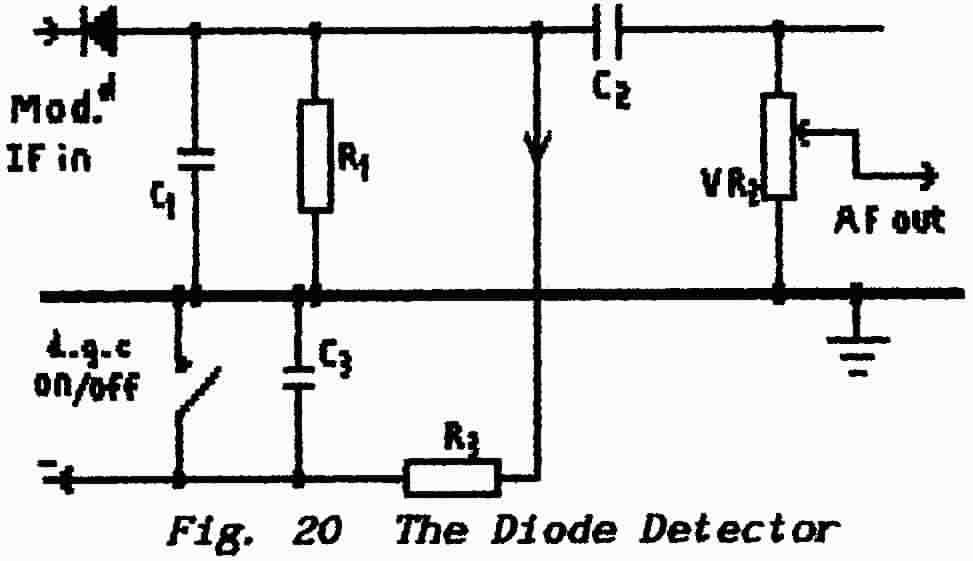 |
** This varying voltage is resolved into a direct component, representing the amplitude of the unmodulated carrier, and an alternating modulation voltage. Capacitor C2 blocks the dc but passes the AF to the Volume control VR2. Resistor R3 and capacitor C3 form a low-pass filter that permits only the direct-voltage to pass to the a.g.c. line. |
** As always the values of the different components has to be a compromise between conflicting requirements. If the leak resistor Ri is made too small the capacitor will discharge too much and so cause an if-frequency ripple to appear and the audio output may not follow the increases in carrier amplitude. If the leak is made too large the capacitor will discharge too slowly for the output voltage to follow the decreases in carrier amplitude. Capacitor C2 has to be large enough to pass the lowest audio frequency but not so large that it passes also the variations in direct-voltage caused, for example, by signal fading. The time-constant of C3,R3 is less critical but it must remove both the rf and audio frequencies from the a,g.c. line without reducing the slower variations caused by fading.
** Diode detectors produce distortion of the modulation waveform because the load presented to them varies with frequency. For the dc component of the diode output the diode load consists of the resistor R1. For the audio component the load consists of R1 in parallel with VR2 for those frequencies which pass C2. At lower frequencies the coupling capacitor introduces phase shift also. This difference in loading leads to waveform distortion when the modulation index approaches 100% and this is the reason why a.m. transmitters are adjusted for a maximum modulation depth around 80%.
A detector accepts an rf-signal input but produces an output at audio frequencies. The manner in which it converts one to the other is often
>>>>>>>>>>>>>>>>>>>> PAGE 34 <<<<<<<<<<<<<<<<<<<<
expressed as a transfer characteristic. For distortion-free detection this transfer-characteristic should be linear (i.e. a straight line which indicates that the output is directly proportional to the input). For very-low input signals, which are only just able to drive the diode into conduction, this characteristic tends to a square law ; i.e. the audio-output varies as the square of the if input. In this mode the arrangement is referred to as a square-law detector. To ensure linearity the diode should produce about 1-volt which, apart from selectivity, is the main reason for pre-detector amplification.** For a communications receiver there is one other facility required and that is an A.G.C. On/Off switch. It can be useful to remove the a.g.c. when a signal, although weak, nevertheless exceeds the delay voltage and reduces the gain. The main purpose of this switch however is that, in cw mode, the B.F.O. signal generates a substantial a.g.c. voltage which obviously precludes the reception of any but the strongest signals.
END OF LESSON 5
* * * * * * * * * * * *
QUESTIONS
1. What are the differences between an rf-amplifier and an if-amplifier ?
2. In modern circuits why are the connections to active devices taken from (and to) tapings on the coils ?
3. What is the purpose of a.g.c. ? In which particular circuits would you not expect to find such a facility ?
4. In the text (page 31) it is suggested that if-transformers are tuned by means of trimmer capacitors. How else could tuning be achieved and can you point out a problem that could arise ?
5. What is critical-coupling and why is it not necessarily the ideal ?
6. A bandpass coupled-pair is constructed from two separate coils which are coupled through a small variable capacitor. At each end the capacitor connects to a tapping one-quarter of the way up each coil from the earthy end. What would be the effect on the capacitor if both tapping-points were moved to the centres of the coils ? (NOT for R.A.E.]
7. Why do communications receivers require an A.G.C. On/Off switch ?
8. What is the purpose of "delayed a.g.c." ?
9. In a diode detector circuit why would you suspect that the load-resistor had become open-circuited ? How could you check this using a meter ?
>>>>>>>>>>>>>>>>>>>> PAGE 35 <<<<<<<<<<<<<<<<<<<<
** As already described a discriminator first puts the frequency-modulated signal through a frequency-conscious network which transforms it into a carrier that is simultaneously frequency-modulated and amplitude-modulated. The audio waveform is then extracted with a diode as is done with an a.m. signal.
Perhaps the simplest way to achieve this is to detune an rf-amplifier until the carrier frequency lies about half-way down the skirts of the frequency characteristic (see lower diagram in Fig. 19 of Lesson-5). With the receiver adjusted in this manner the rf output increases as the carrier-frequency moves toward the tuned-circuit resonance but decreases as the carrier-frequency swings in the opposite direction.
An fm transmission can be read in this fashion if all else fails but it is seldom very satisfactory. (Switch-off the a.g.c.!) The obvious problem is the lack of linearity ; i.e. the lack of a direct relation between the carrier excursion (or deviation) and the amplitude of the output signal because the characteristic is curved.
|
The next simplest consists of two separate tuned circuits one tuned to the desired upper frequency-limit and the other tuned to the desired lower frequency-limit. As shown in Fig.21 each circuit has its own diode detector but they are connected, in opposite sense, to a common load. |
The outputs from the diodes cancel and so, when the carrier frequency passes through its un-modulated value fc , the output voltage developed across the load-resistor R is zero. When the carrier-frequency swings toward the resonance-frequency of the upper tuned-circuit then the positive output from diode Dl is greater than the negative output from diode D2 and so the output is positive. Conversely, as the carrier-frequency swings toward the resonance-frequency of the lower tuned-circuit, then the negative output from diode D2 predominates and so the output is negative. The overall effect is illustrated in the graph alongside.
This type of circuit does not produce a dc-component which represents the carrier amplitude because, at the centre frequency, the diode outputs sum to zero.
This simple arrangement produces a much better linearity than the de-tuned rf amplifier described above but it is not easy to get it to align so that it gives both good linearity (low distortion) and also a reasonable sensitivity. However the arrangement has been used in refined form to demodulate f.m. signals in the uhf band and above and it was once used as a cheap sensing circuit to drive motorised tuning devices.
>>>>>>>>>>>>>>>>>>>> PAGE 36 <<<<<<<<<<<<<<<<<<<<
** Discriminator circuits such as the Foster-Seeley and the Ratio Detector provide much better linearity . The ratio-detector is the more common these days because it provides discrimination against carrier-amplitude variations (a.m.) ; for this reason it is not unusual to see a ratio-detector used without a limiter stage.
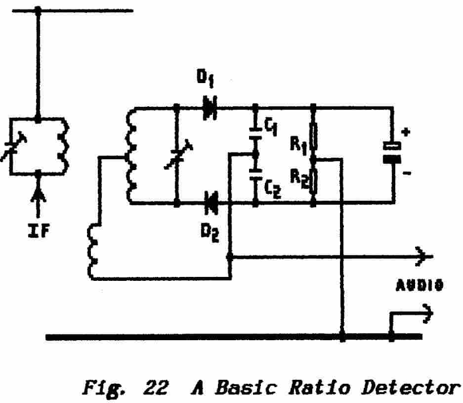 |
** The ratio-detector is shown in Fig.22
; it is easily distinguished from the Foster-Seeley
by the reverse-connected diodes. Both discriminators derive quadrature
samples of the incoming carrier and produce signals which are the sum
and the difference of these two.
** The final if-transformer is double-tuned in the normal bandpass arrangement but the secondary is centre-tapped. A portion of the primary voltage is tapped-off by a tertiary winding ( a capacitor could be used) and fed to the centre of the secondary. Either coupling component provides a 900 phase-shift. Thus the two diodes are fed (a) with primary-signal plus secondary-signal and (b) with primary-signal minus secondary-signal. |
** At the centre-frequency, where both tuned circuits are resonant, the outputs from the two diodes are equal, the load capacitors Cl and C2 are charged to equal voltages and a direct potential is developed across the two resistors R1 and R2. In operation this potential changes very little and so a large-value capacitor (2 to10 µF) can be connected across the circuit and it is this that provides the immunity to carrier-amplitude changes.
** As the carrier-frequency swings about the resonance-frequency so the phase of the secondary signal shifts. This causes the voltage applied to one diode to increase as the voltage applied to the other decreases. As a result the charges on Cl and C2 vary and the potential of their centre point varies with the modulation waveform. The Ratio Detector derives it name from the fact that the audio signal depends on the ratio of the voltages across the two load capacitors.
** The audio signal can be obtained across either Cl or C2 but such an arrangement would upset the rf balance of the circuit. It is better to tap the resistive load at its centre (hence R1 = R2) to provide the earth-connection. (Note that the circuit as drawn in Benbow's RAE Manual is not wrong but is drawn deceptively ; the upper of his two audio connections is earthy.]
N.B. You should understand the ratio-detector but you will not receive any searching questions about the details of its operation.
>>>>>>>>>>>>>>>>>>>> PAGE 37 <<<<<<<<<<<<<<<<<<<<
** The term ssb is the accepted form for suppressed-carrier single-sideband transmissions and the first step in recovering the modulation information is to re-insert the carrier. This must be achieved with an accuracy of at least 25 Hz.
** In an ssb receiver the required carrier signal is generated in a carrier-insertion oscillator (c.i.o) but, as already discussed, it is possible in a communications receiver to use the b.f.o. for this purpose. The carrier level required to demodulate an ssb signal however is fairly large while that required from a b.f.o. for cw reception is small. To demodulate ssb successfully with a normal communications receiver it is necessary to juggle with the RF-Gain, Aerial-Attenuator and AF-Gain controls; where they are fitted the Bandwidth and IF-Shift can be useful too.
As discussed in Lesson-3 of Part-2 there are two methods of heterodyning signals namely add them or multiply them. Simply adding two signals (or mixing them) results in a beat which has to be extracted (or detected) by use of a rectifying diode. This is the method used when the bfo is employed in a normal communications receiver. Multiplying one signal by another yields the sum and difference frequencies directly and this is the method used in the so-called Product Detector.
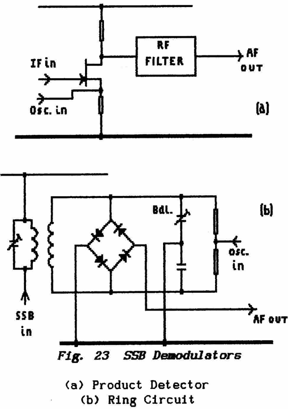 |
** A basic circuit for a product detector
is shown in Fig. 23(a). Essentially this is a
simple common-source amplifier stage with separate inputs to the gate and
source. The current which flows between source and drain is controlled
by both input signals with multiplicative effect. The audio output is taken
from the drain via an rf-filter.
** The Ring Modulator shown in Fig.23is an example of additive mixing. The four diodes are connected in a continuous ring formation (compare this with the bridge-formation in Part-5). The circuit is exactly the same as the Ring Modulator used in transmitters to achieve ssb but here it is used in a "reverse" sense. Instead of putting-in an audio and a carrier and recovering a ssb signal, here we put-in a ssb signal and a carrier and recover the audio. Analysis of these circuits is not required for the R.A.E. but, for those who are curious, the easiest way to understand them is to regard the diodes as switches which are operated in pairs by the inserted carrier. The ssb signal is directed through the audio load in a series of pulses at if-rate which are smoothed out by an rf-filter into the audio waveform. |
>>>>>>>>>>>>>>>>>>>> PAGE 38 <<<<<<<<<<<<<<<<<<<<
** The fact that a ring circuit can be used for both modulation and demodulation means that it is often found in Transceivers where it is switched between the two modes for either transmitting or receiving purposes.
** The product detector too has its advantages because it can demodulate both ssb and cw signals with the same low-level input from a local oscillator.
** The b.f.o. operates over a small range of frequencies centred on the i.f. Frequency-adjustment is by means of a front-panel control which enables the operator to set the audio output frequency either to a preferred note or so that he can the more easily discriminate between a wanted signal and an unwanted signal.
** This second reason is the main purpose of the b.f.o. control. Rocking the receiver main-tuning control affects the frequency of the carrier delivered to the i.f. section (from the frequency-changer) and so, in general terms at least, a fixed-frequency b.f o. is sufficient as far as the audio note is concerned.
** The b.f.o. control normally gives some 3-kHz adjustment both above and below the intermediate frequency. This provides two possible settings for the b.f.o. to produce a given audio output but, while one of these settings produces a high-frequency audio beat with an interfering signal, the other setting must produce a low-frequency beat with that interfering signal. Of course, if the interfering signal is exactly on the frequency of the required signal, it is not possible to separate them.
Skilful use of the b.f.o.-control, of the bandwidth-control, of the if-shift control and of the main tuning (in combination) can often eliminate an unwanted cw signal.
** Any of the oscillator circuits described in Part-4 of this Course can be used for the b.f.o. Generally it is desirable to keep its output at as low a level as possible else it generates a large a.g.c. signal and so reduces the receiver gain ; an a.g.c. switch is an alternative here. The oscillator should be well screened, decoupled and filtered to prevent it adding its quota to the traditional family of howls and squeals that can beset superhet receivers.
You are not required to produce circuit details of noise-limiting circuits for the R.A.E. which is just as well because most of them seem to be little more than decorative knobs for the front panel.
** Most intrusive noises consist of large-amplitude and wide-spectrum spikes caused by such things as lightning, car-ignition circuits, switching surges and "splashes" or the continuous noise from electric brush-motors.
>>>>>>>>>>>>>>>>>>>> PAGE 39 <<<<<<<<<<<<<<<<<<<<
** Spikes are dealt with by using biased diodes to clip-off that part of the spike which exceeds the amplitude of the wanted signal ; these are known as clipper circuits. The idea is that, when the signal+noise exceeds the bias voltage, the diode is driven into conduction and reduces the circuit gain. That part of the spike which is left embedded in the signal cannot be dealt with. The clipping-level can be adjusted by making the diode bias variable.
To describe the action of these clippers is often a matter of preference ; sometimes the conducting diode provides a shunt path that diverts current from the input to a transistor, sometimes it connects a secondary resistor in parallel with a load resistor and so reduces the circuit gain, sometimes it connects the signal circuit to a low-impedance (a constant-voltage) direct-voltage source so that, for the duration of the pulse, the signal amplitude is held constant ; this last circuit-arrangement is often referred to as a clamp.
There was a pulsed form of interference known as "woodpecker" which seemed to stem from some sort of Russian radar and which presumably will not be heard again now that Russia has undergone a change of policy. I have not discovered how the anti-woodpecker noise-limiters are supposed to work which probably explains why they have never worked for me.
Continuous noise such as that caused by arcing at the brushes of rotating machinery cannot be dealt with by noise limiters in radio receivers. However, if the interference is severe in that its peaks exceed the amplitude of the signal, then of course its effect can be mitigated by a diode-clipper circuit. Motor noise must be dealt with at source as described in Part-6 of this Course. Often a cure (at source) can be effected, where arcing is occurring at switching points, by use of the constant-resistance network which is described in Part 8: Information Sheets; No.10.
** Again circuit details are not required for the R.A.E. Especially in f.m. receivers the output consists of a large-amplitude hiss when a carrier is not present at the input. This is because an a.g.c. signal is not being generated or the limiter stage is not in operation and so the receiver operates at full gain.
** A squelch circuit is intended to obviate the nuisance of such noise by using a diode with variable bias (or some similar "threshold device") to shut-off the receiver audio circuits until a carrier appears. (Note that the squelch cannot operate on the rf-circuits.) The squelch bias is set so that the receiver "opens-up" on receipt of a signal.
Some people seem to think that a squelch can be adjusted so as to reduce the background noise level when working with a very weak signal but this is not true. The squelch needs to have an adjustable threshold to prevent a weak unwanted signal continually opening the receiver but a wanted signal has to be either strong enough to operate the squelch or too weak to do so. A weak borderline fading signal may in fact trigger the squelch intermittently and then the only cure is to switch-off the circuit and rely on the ear to sort the signal from the noise.
>>>>>>>>>>>>>>>>>>>> PAGE 40 <<<<<<<<<<<<<<<<<<<<
** Nearly all communications receivers have a front-panel S-meter whose primary function is to indicate the received signal-strength. As a secondary function it serves to indicate the point of accurate tuning, when the signal-strength has reached a maximum value, but this is often a snare and delusion because the signal is fading. In transceivers the meter doubles also as a monitoring device which aids in transmitter adjustments.
For fm reception a tuning meter needs to operate with a centre-zero to indicate the correct tuning point so that, when the carrier is at its unmodulated frequency, the meter does not deflect; see Fig. 21. The meter must be switched from the discriminator output to measure the bias developed in the limiter stage if an indication of signal-strength is required.
The range of input signal to a receiver can be enormous ranging from a few microvolts up to even a volt if a powerful transmission is arriving from a nearby location. To compress such a range within the scale of a meter it is necessary to use a logarithmic law (see Part-7: Mathematics). This means that the meter-deflection is not proportional to the signal strength but to the logarithm of the signal-level change and so the scale is calibrated in terms of decibels.
However it is not necessary to use expensive meters whose magnetic fields have been tailored to a logarithmic law because the receiver itself supplies the necessary characteristic when a.g.c. is in use. Note that an S-meter does not function when the a.g.c. switch is set to OFF..
The a.g.c. signal causes the current drain of the receiver to fall and, if this current is passed through the meter, an indication of signal strength is obtained. Unfortunately the meter reduces its deflection as signal strength rises. There are many circuit arrangements which can be used to reverse the meter action but an alternative is to arrange for the meter to indicate the magnitude of the a.g.c. signal.
The a.g.c. characteristic seldom shows a good logarithmic law except for a part of the signal range and, for this reason, an S-meter is not a reliable indicator of incoming signal strength. There is no reason of course, if you have a suitable signal generator, why an S-meter cannot be calibrated.
In high-quality equipment however you may find circuits which tailor the meter response to improve the law. That part of a diode characteristic where the current is low (just after conduction begins) is usually a very good logarithmic law ; an improved characteristic can be obtained just by shunting a meter with a diode and, probably, by adding a suitable resistor in series either with the meter or with the diode.
The circuit which drives the meter from the a.g.c. line may also be loaded with a series of diodes with graded biases so that, as the signal-strength increases, the diodes progressively come into conduction and modify the meter response.
>>>>>>>>>>>>>>>>>>>> PAGE 41 <<<<<<<<<<<<<<<<<<<<
Sometimes a.g.c. may be taken from the audio output. In such an arrangement a bridge rectifier (see Part-5) is used to obtain a dc-signal from the af-signal. This does not materially affect the action of any S-meter.
** When two circuits share a common impedance, such as the internal-resistance of a power-supplier or battery, then they are coupled together by that common-impedance and unfortunate feedback effects can occur. For example, a large-signal stage which is drawing a large signal-current can develop a signal-voltage across the power-supplier. When that supplier is also the auxiliary supply for an earlier smell-signal amplifier then an amplified signal is fed-back from the output-stage to the small-signal input stage and oscillation can result.
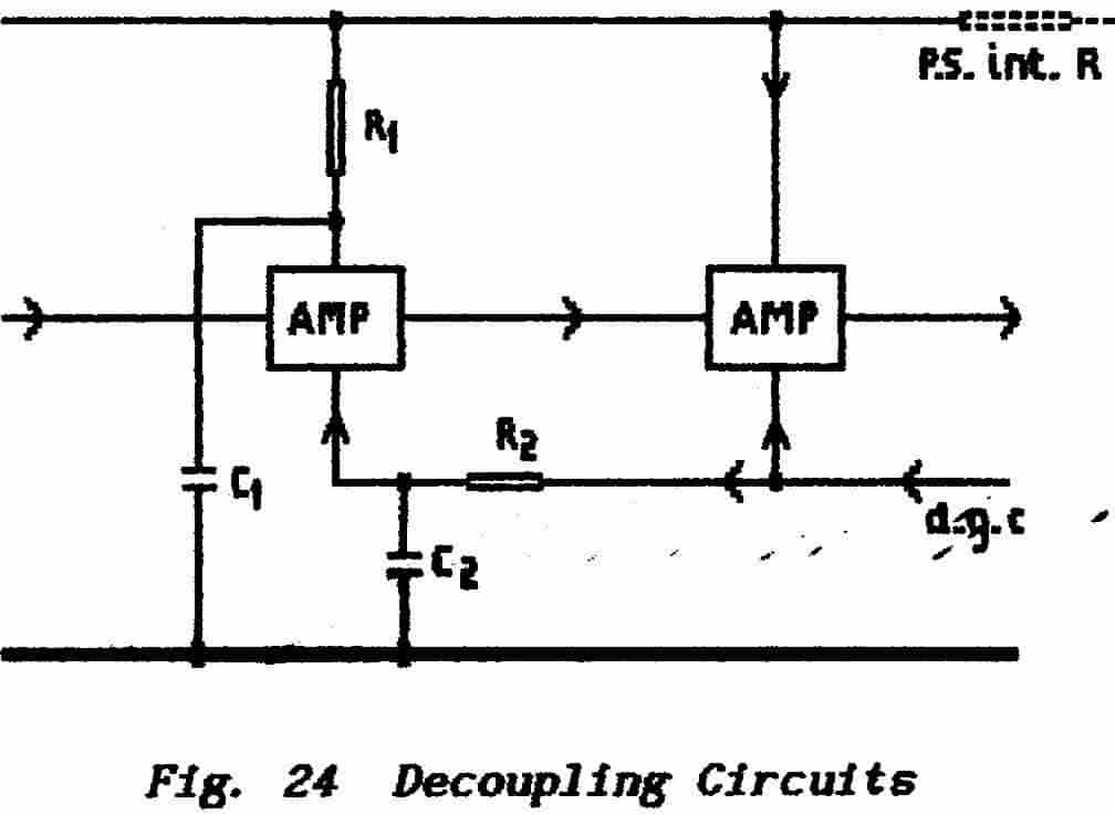 |
** Fig. 24 shows
the above arrangement in block form with a stage of decoupling inserted
to isolate them against this kind of feedback. The time-constant C1R1 seconds
(C in Farads, R in ohms) must be large with respect to the period(time
for one cycle) of the lowest frequency which can pass through the
amplifier.
More decoupling is shown also in the a.g.c. line to prevent unwanted feedback via this route. ** Briefly the capacitor provides a-low-impedance path to ground for any feedback signals while the resistor raises the impedance of the alternative path. |
Many modern receivers are fitted with a notch filter whose rejection frequency can be adjusted by means of a front-panel control. Its use in reducing an unwanted signal in cw-working is obvious. The IF-shift control is perhaps a little more mysterious. It affords a means of sliding the if bandpass-characteristic along the spectrum so that, for example, an interfering signal can be "pushed over the edge" of the pass band and so attenuated without affecting the wanted signal. It can be very effective when used in combination with the notch filter.
In practice the if-passband is not itself moved. The control drifts the local-oscillator frequency so that all the signals that emerge from the frequency-changer within the if band are moved with respect to the passband. It matters not whether the group of signals or the passband is moved; the effect is the same.
>>>>>>>>>>>>>>>>>>>> PAGE 42 <<<<<<<<<<<<<<<<<<<<
An Active Filter is one which includes an active device because this enables it to perform in much the same manner (or even better) than an LC filter but without the bulky (and lossy) presence of inductors. While it is convenient to talk about "artificial" inductors there is in some instances a subtle difference. Operational-amplifiers (Op-amps) are used in conjunction with capacitors to produce inductor-like effects in that the current lags the applied voltage ; such a circuit can resonate with an external capacitor to produce the many different forms of LCR filters.
A circuit arrangement known as a Gyrator converts a capacitive reactance to a genuine inductive reactance ; alternatively the negative-impedance converter changes a capacitive reactance to a negative-inductive reactance which means that, although the current lags the voltage as required of an inductor, the reactance of the circuit falls as frequency increases in the manner of capacitive reactance.
Active filters can be made in low-pass, high-pass, bandpass, band-stop and tunable forms and are particularly useful in audio circuits. In addition an "all-pass" filter can be made ; this offers a flat frequency-response but controls phase-shift (also known as a delay-equaliser).
The Op-amp is manufactured as a chip, smaller in size than a postage stamp, with an enormous open-loop gain (i.e. gain before the application of feedback). Op-amps come also in dual and quad forms in which a single chip offers either two or four completely separate and often matched op-amps. With gains up to one-million-times between two points less than a half-inch apart stray couplings can spell trouble and so circuit lay-out can be as important as the electronic design.
They are offered as "general-purpose" types and also designed for specific purposes such as high-quality audio amplifiers. Their construction may use standard bipolar-transistor technology or the more fragile MOSFET technology which features very-low power consumption ideal for battery-operated equipment.
They are usually operated from a split supply( i.e. between a positive-rail and a negative-rail) but some types are capable of operating from single-ended supplies and some obliging types can cope with either.
They all have three features in common:
(a) they are dc-coupled
(b) they are intended to be used with large amounts of negative-feedback
(c) they have two differential input terminals labeled " + " and " — " but this does not indicate electrical polarity. An input-signal applied to the " + " terminal appears at the output in the same non-inverted form while the same signal applied to the " — " terminal appears at the output inverted.
>>>>>>>>>>>>>>>>>>>> PAGE 43 <<<<<<<<<<<<<<<<<<<<
Note that, if a signal is applied simultaneously to both input terminals, then cancellation occurs and the output is zero; this is exploited in some audio op-amps to provide a control of signal amplitude.
The internal circuitry of these op-amps is very complex and a "gain" control as such is not available except by variation of the external feedback circuit.
Detailed knowledge of op-amp operation is not required for the R.A.E. However the devices feature in many of the projects which appear in amateur-radio publications and a short description of their basic operation follows.
The internal circuitry of op-amps employs 20 or more transistors so that the overall voltage gain is normally in the range 105 to 106 . This means that it requires only a few microvolts (applied between the differential inputs) to swing the output terminal between the extreme limits of the power supply.
When negative-feedback is applied to an op-amp these enormous gains mean that the behaviour of the circuit is controlled almost entirely by the characteristics of the feedback loop.
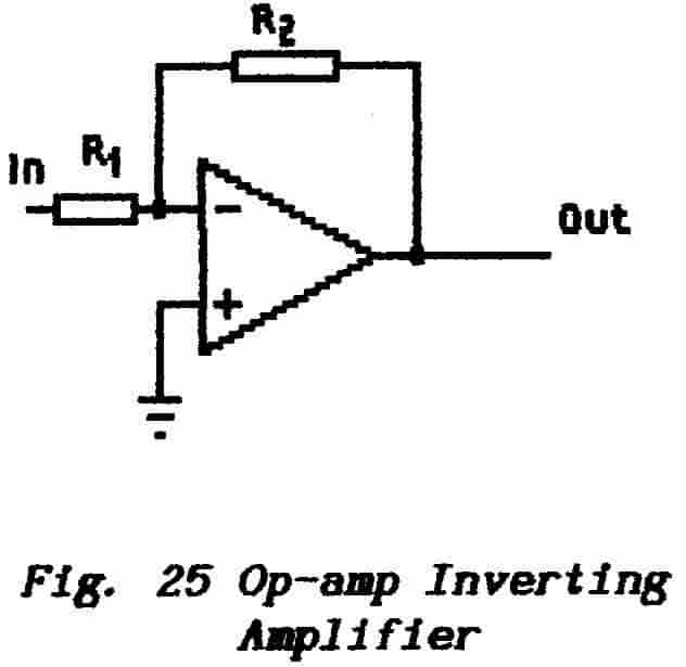 |
Fig. 25 shows an op-amp connected as an inverting amplifier which means only that, whatever else it does to the signal, it also turns it "upside down". Note that the standard symbol does not show the connections from the chip to the positive and negative rails of the power-supplier. The resistor R2 is the feedback path through which the output voltage drives a current which cancels the input current arriving through R1. The input-voltage developed between the two input-connections is only a few microvolts and is negligible when compared with the voltage developed across R1. For practical purposes therefore the input-voltage appears across R1 and so this resistor defines the input-impedance of the amplifier. |
For those with a bent for algebra it is not difficult to show that the voltage-gain of this circuit is given by the ratio R2/R1
In stating that the input voltage between the " + and " — " terminals is negligibly small we are saying that the feedback action (in practical terms) ties the two inputs together. With the " + " terminal taken to earth it follows that the"-" terminal is also very close to earth potential and this is described as a virtual earth.
When such an amplifier is required to provide a fairly high gain the value of R1 becomes small and consequently the input-impedance is small.
>>>>>>>>>>>>>>>>>>>> PAGE 44 <<<<<<<<<<<<<<<<<<<<
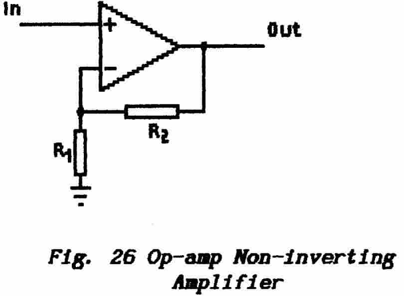 |
Input impedances up to
1012 ohms or higher are possible with the non-inverting amplifier
shown in Fig. 26.
For both arrangements the output impedance is a fraction of an ohm. |
The above can be summarised as two rules:
1. The operation of the feedback loop ensures that the output settles at a value which brings the two input terminals to (nearly) the same potential.
2. The small pd developed between the two input terminals means that the input current (to the op-amp proper) is (almost) zero.
Op-amps, op-amp circuits and their applications are multitudinous and beyond the scope of these Lessons. However, should any reader be presented with a problem, I will be pleased to advise.
END OF LESSON 6
* * * * * * *
QUESTIONS
1. Describe briefly how a ratio-detector demodulates an fm signal.
2. What would you expect a product-detector to do
3. What are the various uses to which a b.f.o. may be put ?
4. An f.m. receiver (e.g. a C.B. rig) remains obstinately quiet. Suggest a reason and appropriate remedial action.
5. What is the first essential in detecting an ssb signal ?6. A superheterodyne receiver operates over the range 14 to 15 MHz. If the i.f. is 10.7 MHz what range will the local oscillator have to cover ?
7. In an amplifier stage what components would be associated with a bipolar transistor which would not be present with a FET ?
8. What is automatic bias? Where would you find the appropriate components in an amplifier circuit ?
END OF PART 3
Back to Top of Page
>>>>>>>>>>>>>>>>>>>> PAGE 45 <<<<<<<<<<<<<<<<<<<<